
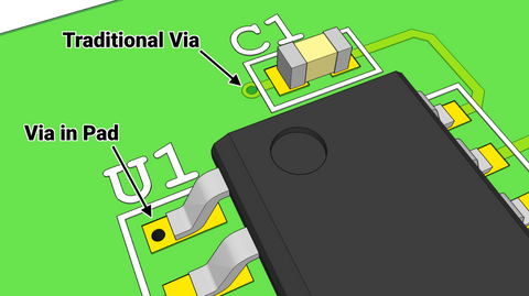
Via-in-pad is the design of placing the via inside the copper pad, and it is usually used for space optimization of the PCB. The PCB can provide up to 50% space for placing components when using via in pad technology. The pursuit of finer pitch devices and smaller electronic products has led to the widespread use of via in pad by PCB engineers.
We know that other vias such as buried vias and blind vias are good at saving space and increasing component density, but via in pad is still the ideal solution for the PCBs with high speed and high dissipation requirement.
The advantages of via in pad in PCB design
1. Reduce PCB volume or size for multi-layered PCBs and high-density PCBs
2. Allow smaller and compact routing
3. Simplify the routing for the LGA package and BGA package
4. Achieve the routing demands for fine or big pitch BGAs easily
5. Reduce the inductance in high-speed PCB designs
6. Better thermal management
7. Increase voltage capability of the vias
8. Provide flat and coplanar surface
9. Helpful for high-frequency components grounding
10. Reduce manufacturing defects and increase yield
11. Reduce the EMF emissions in high-frequency PCB designs
Some considerations about via in pad
Although via in pad routing has various advantages, it does increase fabrication complexity and material cost. Because creating additional vias need to drill more holes, more coppers to plating the hole, and more materials to filling the vias. This process may also cause other problems, such as voids may be formed in the solder joints as the air bubbles migrate upward through the vias.
Therefore, considering the additional manufacturing time and cost required for via in pad routing, it is better to avoid pad in via design if you can achieve your purpose with traditional via routing. If you concern more about compact routing and small board size, via in pad routing is your ideal solution.
And when you design via in pad, you should ensure that the via in pad meets the manufacturer’s minimum annular ring requirements. And additional drill file is needed to manufacture the PCBs with via-in-pad routing technology. There are always different price and lead time with via in pad technology compare to the traditional routing. It is better to let your manufacturer know your demands before you place orders.