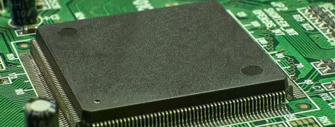
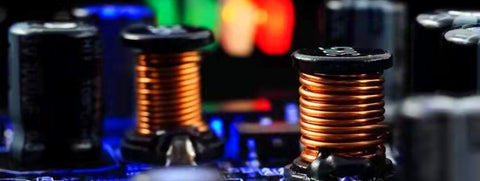
Many newbies will determine the quality of the quality based on the color of the scrap circuit board. So, what effect does the color of the PCB board have on performance?
In fact, the color of the PCB circuit board does not have a great relationship with the performance of the PCB. The color of the surface of the seed pcb is actually the color of the resistor. One is to avoid the conditions for component soldering; the other is to slow down the use of components and avoid oxidation and corrosion in the air of components routing.
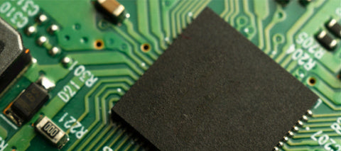
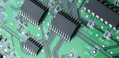
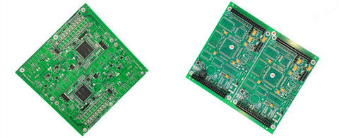
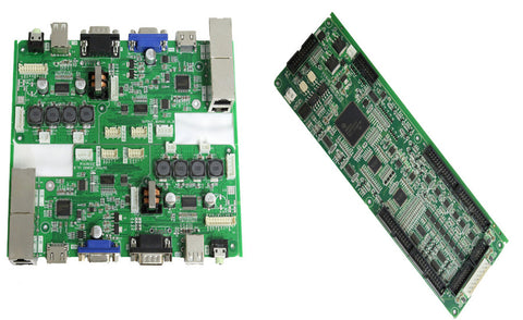
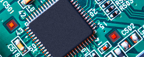
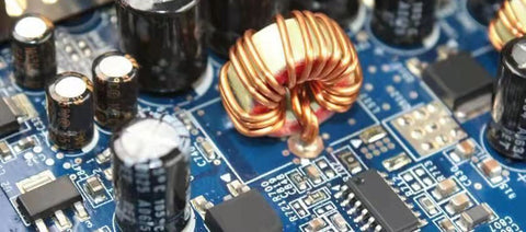
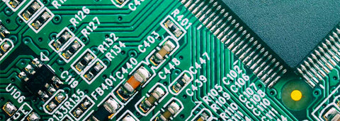
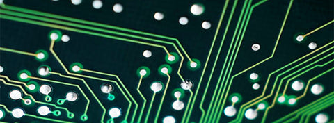
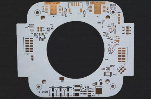
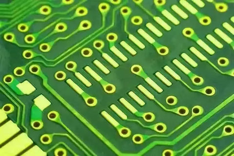
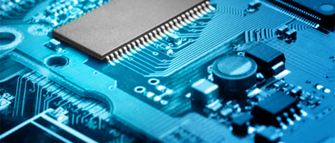
If you have a better understanding of multi circuit boards, you will find that the color of the board is generally green. In addition to green, electric board circuit colors can be said to be varied: white, light yellow, red, dark blue, sub-light, and even chrysanthemum, blue-purple, black, bright green, etc.
In all links from product development to product landing, the color is determined according to the main purpose of the integrated circuit board. The existence of white is because of the product requirements of lighting fixture PCBs, and white applications must be used. Among other colors, electronic test equipment PCB may be blue and purple, electronic computer PCB will be black, etc.
The most common green PCB circuit board, also known as green oil, this is because the green processing process is the most perfect, the simplest, and the lowest cost.
In addition, green oil also has many advantages: the production and processing of metal pcb, the production and manufacture of electronic equipment, including the plate-making process and its plates, in this process, there are multiple processes to go through the white light room, and the green PCB board is in the white light room. The visual impact is the best.
]]>Corresponding inspections are required before and after the complete PCBA processing is completed. So, how to effectively inspect after SMT chip processing?
1. Check the layout of the pcb module board for foreign matter residues, PCB scratches and other undesirable phenomena.
2. The inspection direction is moved from left to right and from top to bottom, and the mounted copper base pcb are inspected one by one.
3. The components should not be missing, wrongly installed, empty welding, etc.
4. The polarity of the components cannot be reversed.
5. The pin displacement of IC, exclusion, transistor, etc. cannot exceed 1/4 of the pad width.
6. The displacement of the Chip component cannot exceed 1/4 of the width of the pad in the parallel and vertical directions.
7. Hold the edge of the high volume pcb and gently place it on the conveyor belt of the reflow soldering machine. Be careful not to drop it from a high place to prevent the components from falling off.
8. Detect the bad small batch pcb, paste the sign paper, and trim and adjust it in time.
9. Other precautions: You must wear an anti-static wrist strap. Take the edge of the PCB during operation, and do not touch the surface of the smt pcb with your hands to prevent damage to the solder paste printed on the pad; during the mounting process, add components Be sure to pay attention to the model, specification, polarity and direction of the components.
]]>There are now more mobile phones and laptops than the entire world population. After using these mobile devices thoroughly, the researchers successfully paired them into final recyclables, resulting in more environmentally friendly devices in electronics manufacturing. Likewise, with the advent of soluble PCBs, there has been rapid innovation in the medical world. Medical research first came up with the idea of an electron-dissolving device: Once dissolved, it’s gone.
In addition, the skilled soluble PCBA concept has led to the medical need for unique technologies including brain monitors, electrical stimulators to accelerate bone development, and drug delivery systems to implant them in the human body.
From insulin pumps to pacemakers, electronic implants are powerful and resourceful health insurance tools. However, they have a range of high risks in terms of surgical complications and health. Soluble PCBA technology emerged with these critical needs of the medical industry. With the new development of the electronics manufacturing industry, its wealth has gradually expanded to important fields such as consumer electronics, recycling technology, and marine industry.
The new PCBA technology supports medical innovation, in addition to supporting robust and improved healthcare in the clinic and hospital field, it operates at various pain points with high-performance patient monitoring capabilities.
Soluble pcb prototypes have created many new discoveries in medical electronics, saving time by avoiding additional surgery, reducing medical complexity, and providing patients with reliable and less painful treatments. As a new field in the medical, healthcare and dental industries, the current trend of high frequency and multi-function is developing, which indicates a significant increase in electronic innovation of printed circuit boards.
Water-soluble flux is one of the various fluxes in PCB assembly that suspends the solder paste process and acts as a medium for eliminating solder particles. It consists of corrosive and reactive organic acids. In mainstream soluble PCB components, it is important to leave and set a critical level of corrosion flux residue on the printed circuit board.
Based on board geometry, material composition, and flux type and volume, flux removal has become a hot topic for successful soluble PCB fabrication. This is because if any flux remains on the board, it can increase the likelihood that the ECM will cause a serious failure. After the reflow process is completed with the flux and water-soluble paste in the PCB, the flux residue is removed thereafter.
Now, soluble PCBAs can meet the exact needs of the complex framework and criticality of brain monitors. These tiny chips that can be implanted into the brain help doctors monitor people who have had brain surgery or head trauma. Soluble PCB assemblies are also a step forward in the retrofitting of neurodiagnostic devices, leading to advances in physiological and brain interpretations related to neurodegenerative diseases, chronic diseases, and patient sleep quality.
]]>
If the budget is not large, but a PCB board with better heat dissipation performance is required, what kind of substrate should be selected? The best answer is aluminum substrate PCB.
The Advantages of aluminum substrate PCB
1. Heat dissipation: High temperatures can cause serious damage to electronic equipment, so it is wise to use materials that help dissipate heat. In fact, aluminum can transfer heat from vital components, thereby minimizing its harmful effects on the circuit board;
2. Environmental protection: Aluminum is non-toxic and recyclable. The use of aluminum also contributes to energy savings due to ease of assembly. For PCB suppliers, the use of this metal helps keep the planet healthy;
3. Lightweight: Aluminum is incredibly durable and is an amazingly light metal. Aluminum adds strength and elasticity without adding any extra weight;
4. Higher Durability: Aluminum provides strength and durability to products that ceramic or fiberglass substrates cannot. Aluminum is a solid substrate that reduces accidental damage during manufacturing, handling and everyday use.
The Application of aluminum substrate PCB
1. The Audio equipment: input and output amplifiers, balanced amplifiers, audio amplifiers, pre-amplifiers, power amplifiers;
2. The Power supply: switching regulator, DC/AC converter, SW regulator, etc.;
3. The Communication electronic equipment: high-frequency amplifier, filtering equipment, transmitting circuit;
4. The Office automation equipment: motor drive, etc.;
5. The Automobile: electronic regulator, igniter, power controller, etc.;
6. The Computer: CPU board, floppy disk drive, power supply equipment, etc.;
7. The Power module: inverter, solid state relay, rectifier bridge;
8. The Lamps and lighting: With the advocacy and promotion of energy-saving lamps, various color energy-saving LED lamps are welcomed by the market, and aluminum PCBs for LED lamps have also begun to be applied on a large scale.
]]>After the SMT patch proofing of the SMT small batch patch processing factory is completed, some follow-up processing procedures, such as testing, assembly, etc., are required. After all the electronic processing links are completed, it is delivered to the customer. The circuit board processed by the SMT patch It is relatively easy to be disturbed by various factors in the delivery and transportation process, such as bumps, collisions, friction, etc.
So how should the smt electronics factory transport it to ensure that the circuit boards processed by SMT are not damaged and reach the customers safely?
The advantages of smt chip processing: high assembly density, small size and light weight of electronic products, the volume and weight of chip components are only about 1/10 of those of traditional plug-in components. Generally, after using SMT, the volume of electronic products is reduced by 40%~60% %, the weight is reduced by 60% to 80%.
The protective measures during the transportation process after the SMT patch proofing are mainly done in the following aspects.
1. Moisture-proof packaging: Before packaging, the surface of the PCB circuit board should be cleaned and dried, and the three-proof paint should be sprayed.
2. Anti-vibration packaging: Put the packaged flexible printed circuit board into an anti-static packaging box. When placed vertically, stack up to no more than two layers, and place a baffle in the middle to keep it stable and prevent shaking.
3. Packaging materials: flex circuit are relatively fragile and easily damaged electronic products, and must be carefully packaged with bubble bags, bubble cotton, electrostatic bags and vacuum bags before transportation.
4. Anti-static packaging: Static electricity will break down the chips welded by SMT on the blank circuit board. Since static electricity cannot be directly observed, it is necessary to use anti-static packaging methods such as electrostatic bags.
Finest Group was established in 2003, and now has 6 new Korean imported (Samsung) dual-track high-speed placement machines, 6 new Korean imported (Samsung) dual-track medium-speed placement machines, automatic printing machine + reflow + online dual-track AOI + SPI + Offline AOI+X-RAY is committed to providing high-efficiency, high-quality one-stop PCBA services for R&D enterprises.
]]>Every PCB assembly manufacturer must adhere to proper cleaning standards. For medical equipment, there is a higher set of cleanliness standards. What are the PCB cleanliness standards that medical devices must meet?
1. Comply with IPC-5704
All medical device development must meet a specific set of quality control standards. Ipc-5704 is a set of standards specifically addressing cleanliness requirements for the manufacture of unassembled printed circuit boards. A large part of this needs to go through the necessary steps to prevent and remove any kind of ionic contamination or other unwanted debris from the Integrated Circuit board.
2. Ultrasonic cleaner
In terms of cleaning methods for prototype pcb assembly manufacturing, this method is the best. This is because ultrasonic cleaning involves a temperature-controlled process that is done at set time intervals. Of course, the solution used in this process will affect the ultimate effectiveness of the method.
3. Automatic cleaning machine
The process involves placing the soldering pcb board in a basket and dipping it into the solution. Once it is taken out of solution, it is then dried. However, it is important to choose a good solution so that any printed circuit board assembly material will not suffer any damage.
4. Manual cleaning
Although rarely used, there is an option to clean printed circuit boards by manual methods. The problem with this approach is that some areas are barely reachable, especially on smaller PCBs. However, for some components, such as the microphone, only the manual method can be used.
The reflow soldering process is a very important process in the welding stage in the small batch processing of SMT proofing. The quality of the small batch processing of SMT proofing depends largely on the welding quality, and the reflow soldering process will directly affect the quality of the patch welding.
Electronic processing plants must continuously optimize the reflow soldering process and improve the soldering quality when processing SMT OEM materials. Circuit board processing enterprises are committed to providing high-quality electronic products and services.
The problems in the reflow process of SMT proofing and small batch processing in the actual process are not only related to this process, but also may be related to many previous processes, such as production line equipment conditions, PCBA substrates The design of pads and productivity, the solderability of components, the quality of solder paste, the processing quality of printed circuit boards and the process parameters of each process of SMT patch processing, etc., are related to the pad design of the circuit board. important connection.
1. Common defects of reflow soldering:
1. The via hole is designed on the pad, and the solder will flow out from the via hole, resulting in insufficient solder paste.
2. When the spacing between the pads is too large or too small, during reflow soldering, since the soldered ends of the components cannot overlap with the pads, a suspension bridge and displacement will occur.
3. When the size of the pads is asymmetric, or the ends of the two components are designed on the same pad, the surface tension will be asymmetrical, which will also cause suspension bridges and displacements.
2. The key elements that should be mastered in the design of integrated circuit board pads: According to the analysis of the solder joint structure of various SMD components, in order to ensure the reliability of the solder joints, the pad design should meet the following elements:
1. Pad width: It should be basically the same as the width of the component end or pin.
2. Pad spacing: ensure the proper overlap size between the component end or pin and the pad.
3. Symmetry: The pads at both ends are symmetrical to ensure the balance of the surface tension of the molten solder.
4. Remaining size of the pad: the remaining size of the component end or pin after overlapping the pad ensures that the solder joint can form a meniscus.
With the development of electronic technology, many electronic products are developing in the direction of miniaturization and precision, and the requirements for SMT chip processing will become higher and higher. Welding requirements and conventional welding process, the welding of components, the main attention is: master the heating time, use the appropriate temperature and good operation.
Welding of different components, in different temperature, air flow and other environments, using different electric soldering irons and soldering iron tips, the skills to be mastered in these three aspects are also different, which requires us to get exercise in a lot of practical operations and improve.
For example, the welding requirements of 0201 SMT components are generally higher than those of 0402. Ensuring the quality of chip welding is one of the processing requirements of electronic processing plants. The quality of solder joints is the core of SMT chip processing. The quality of solder joints is directly related to the quality of this PCBA. So how should the quality of solder joints be detected?
1. Appearance inspection:
1. There can be no missing components;
2. There can be no component paste errors;
3. There can be no short circuit phenomenon;
4. There can be no virtual welding phenomenon.
2. External performance:
1. Good wettability, the edge of the welding point should be thin;
2. The surface of SMT solder joints with good quality is complete and smooth and bright;
3. The appropriate amount of solder and the solder completely cover the soldering parts of the pads and leads, and the height of the components is moderate.
3. Judgment of virtual welding:
1. Visual or AOI inspection.
2. Use special equipment for online tester for inspection.
Fourth, the cause and solution of virtual welding:
1. For PCBs that have been printed with solder paste, the solder paste is scratched and rubbed, which reduces the amount of solder paste on the relevant pads and makes the solder insufficient. should be replenished in time.
2. The pad design is defective. The presence of through-holes in the pads is a major defect in circuit board design. Generally, it is not recommended to use them. Through-holes will lead to the loss of solder during SMT chip processing and cause insufficient solder.
3. The PCB board has oxidation phenomenon, that is, the pad is black and not bright, and the oxidation phenomenon can be removed by an eraser. Generally, when the PCB is damp, the small batch processing factory of SMT proofing is placed in a drying oven for drying. If there are oil stains, sweat stains and other contamination on the board, clean it with absolute ethanol.
Surface wetting of SMT chip proofing refers to a phenomenon when the solder spreads and covers the surface of the metal to be soldered during soldering. The surface wetting of SMT chip processing generally occurs in the case of close contact between the liquid solder and the surface of the metal to be soldered, and only the close contact has sufficient attraction.
When there are contaminants on the surface of the corresponding welded metal, it must not be in close contact. In the absence of contaminants, when the solid material contacts the liquid material in the SMT patch proofing, once an interface is formed, the surface will be reduced. The adsorption phenomenon of energy, the liquid material will spread out on the surface of the solid material, and this is the wetting phenomenon. In the dipping test, the following phenomena are present on the surface of the pattern taken out of the molten solder bath:
1. Partial wetting Some areas of the welded surface are wetted, and some are not wetted.
2. The non-wetting surface is restored to its original appearance, and the welded surface remains the same as before.
3. After wetting and removing the molten solder, the soldered surface will retain a layer of uniform, smooth, crack-free, and well-adhered solder.
4. Weak wetting: The soldered metal surface of the SMT patch proofing is wetted at the beginning, but after a period of time, the solder will shrink from part of the soldered surface to droplets and finally leave only a thin layer of solder in the weakly wetted area .
FINEST provides a one-stop PCBA manufacturer platform, SMT patch, PCB proofing, DIP welding processing, PCB board making, a full set of electronic components purchasing, and some purchasing one-stop PCBA manufacturing services.
]]>The solder paste printing machine is an indispensable processing equipment in the SMT small batch chip processing factory. The quality of the solder paste printing can directly affect the quality of our SMT chip processing.
Now in many processing plants, automatic solder paste printing machines are more and more used in industrial production. When the automatic solder paste printing machine is used for a long time, the equipment will also face the problem of aging and rust. Therefore, we should pay special attention to the maintenance of automatic solder paste printing machine equipment.
In the actual patch processing, the production quality will be interfered by many factors, such as solder paste quality, processing parameters, temperature and humidity, equipment accuracy, etc., and many of these factors will be related to the equipment. Only by ensuring the quality and reliability of the equipment can we ensure that the processing quality is reliable. The equipment is in operation every day, and daily maintenance and maintenance work is very important.
Maintenance method of solder paste printing machine in SMT small batch chip processing factory.
1. Check and clean the stencil, clean the sample, remove the scraper, use a special wipe dipped in absolute ethanol, wipe the scraper clean, and then install it in the printing head or in the receiving tool cabinet.
2. There are two ways to clean the template
1. Washing machine cleaning. Use the template to wash the equipment, the cleaning effect is the best.
2. Manual cleaning. Apply anhydrous ethanol with a special wipe to remove the solder paste. If the leak is blocked, use a soft toothbrush instead of a hard needle. Use a compressed air gun to remove any residue from the template leaks. Load the stencil on the placement machine, otherwise receive it in the tool cabinet. Note: The sequence of removing the template and scraper is to first remove the scraper and then the template to prevent damage to the scraper.
The daily maintenance and maintenance quality of the automatic solder paste printing machine directly affect the service life and product quality of the printing machine. It is necessary to formulate a working specification for the automatic solder paste printing machine so that the smt operator can operate according to the specification.
]]>How to Avoid PCB Soldering Defects?
1. The solderability of the pcb circuit board holes affects the soldering quality
The poor solderability of the circuit board holes will cause virtual welding defects, affecting the parameters of the components in the circuit, resulting in unstable conduction of the components and inner layers of the multi-layer board, causing the entire circuit function to fail.
2. Welding defects caused by warpage
Circuit boards and components are warped during the welding process, and defects such as virtual welding and short circuits are generated due to stress deformation. Warpage is often caused by an unbalanced temperature between the upper and lower parts of the board. For large PCBs, warping will also occur due to the board’s own weight falling.
Ordinary PBGA devices are about 0.5mm away from the printed circuit board. If the device on the circuit board is large, the solder joint will be under stress for a long time as the circuit board cools down and returns to its normal shape. If the device is raised by 0.1mm, it is enough to cause Weld open circuit.
3. The design of the fr4 pcb board affects the soldering quality
In terms of layout, when the size of the circuit board is too large, although the soldering is easier to control, the printed lines are long, the impedance increases, the anti-noise capability decreases, and the cost increases; if it is too small, the heat dissipation decreases, the soldering is difficult to control, and adjacent lines are prone to appear. Mutual interference, such as electromagnetic interference of circuit boards, etc. Related recommendation: What problems should be paid attention to when drawing PCB from the welding point of view.
To sum up the above, in order to ensure the overall quality of the PCB board, in the production process, it is necessary to use excellent solder, improve the solderability of the Electronics PCB board, and prevent warpage to prevent defects.
The common detection methods of PCB Circuit boards in the production process are as follows:
1. Manual visual inspection of 94v0 PCB board
Using a magnifying glass or calibrated microscope, operator visual inspection to determine if a circuit board is out of order and to determine when corrective action is required is the most traditional inspection method. Its main advantages are low upfront cost and no test fixtures, while its main disadvantages are human subjective error, high long-term cost, discontinuous defect discovery, difficulty in data collection, etc. At present, this method is becoming less and less feasible due to the increase in PCB production and the shrinking of the wire spacing and component volume on the PCB.
2. High level circuit boards online test
Through the inspection of electrical performance to find manufacturing defects and test analog, digital and mixed-signal components to ensure that they meet specifications, there are several test methods such as bed of needles tester and flying probe tester. The main advantages are low cost of testing per board, strong digital and functional test capabilities, fast and thorough short and open testing, programmable firmware, high defect coverage and ease of programming, etc. The main disadvantage is that it requires testing fixtures, programming and debugging time, high cost of making fixtures, and difficulty in use.
3. Printed circuit boards function test
Functional system testing is to use special testing equipment in the middle and end of the production line to comprehensively test the functional modules of the circuit board to confirm the quality of the circuit board. Functional testing can be said to be the earliest automated testing principle, which is based on a specific board or specific unit and can be done with a variety of devices. There are types such as final product testing, state-of-the-art mockups, and stacked testing. Functional testing usually does not provide in-depth data such as foot-level and component-level diagnostics for process improvement, and requires specialized equipment and specially designed test procedures. Writing functional test procedures is complicated, so it is not suitable for most circuit board production lines.
4. Automatic optical inspection
Also known as automatic visual inspection, it is based on optical principles and comprehensively adopts various technologies such as image analysis, computer and automatic control to detect and process defects encountered in production. It is a relatively new method for confirming manufacturing defects. AOI is usually used before and after reflow and before electrical testing to improve the pass rate of electrical processing or functional testing. At this time, the cost of correcting defects is much lower than the cost of final testing, often up to ten times.
5. Automatic X-ray inspection
Using the difference in the absorption rate of X-rays by different substances, see through the parts that need to be inspected and find defects. It is mainly used to detect ultra-fine pitch and ultra-high density circuit boards and defects such as bridging, chip loss, and misalignment generated during the assembly process. It can also use its tomography technology to detect internal defects in IC chips. It is currently the only way to test BGA soldering quality and shadowed solder balls. The main advantage is the ability to inspect BGA soldering quality and embedded components, no fixture cost; the main disadvantage is slow speed, high failure rate, difficulty in inspecting reworked solder joints, high cost, and long program development time, which is a newer inspection. method, remains to be further studied.
6. Laser detection system
It is the latest development in PCB testing technology. It scans the printed board with a laser beam, collects all measurement data, and compares the actual measurement to preset acceptance limits. This technique has been proven on bare boards and is being considered for assembly board testing at a speed sufficient for mass production lines. Fast output, no fixture required, and visually unobstructed access are its main advantages; high initial cost, maintenance and usage issues are its main disadvantages.
7. Size detection
Use the two-dimensional image measuring instrument to measure the hole position, length and width, position and other dimensions. Since the soldering pcb board is a small, thin and soft type of product, it is easy to deform in contact measurement, resulting in inaccurate measurement. The two-dimensional image measuring instrument has become the best high-precision dimensional measuring instrument. After being programmed, Sirui’s image measuring instrument can realize fully automatic measurement, which not only has high measurement accuracy, but also greatly shortens measurement time and improves measurement efficiency.
PCB product testing is a critical step in ensuring surface mount reliability. With the continuous development of PCBA manufacturing industry and the increasing improvement of core technologies, the assembly density of shape memory alloys is also increasing, which not only brings about fine lines of circuit patterns, fine pitch of patches and non-visual characteristics of component pins.
The change also brings some challenges to the quality control of PCBA products. At the same time, in the production process of PCBA, how to judge the quality of circuit printed board is becoming more and more important.
The method of acceptance of pcb quality:
PCB circuit board quality acceptance should include design, process, and comprehensive approval. Generally, we should make samples first, test welding, seal samples and then supply in batches, which includes two aspects.
First: the electrical connection performance inspection, usually by the PCB manufacturer self-inspection, the test instruments used are:
① Optical board tester (on-off tester), which can measure the on and off of the connection, and whether the logical relationship of the multi-layer board including the metallized hole is correct;
②Graphic defect automatic optical tester can check the comprehensive performance of flexible aluminum pcb, including lines, characters, etc.
Second: Process inspection, including welding circuit board appearance, finish, flatness, clarity of characters, resistivity of vias, electrical properties, heat resistance, solderability and other comprehensive properties to judge whether it can be accepted.
The development path of SMT proofing and small batch processing has developed rapidly towards the direction of high density. With the development of electronic technology, the market also requires more miniaturization and precision of electronic products. Nowadays, the technology of SMT chip processing is more and more widely used in the electronic industry. In order to realize the miniaturization of electronic products, make them thinner and lighter, and have more versatility, the requirements for the design of circuit boards are now required. More and more strict, the technical requirements are getting higher and higher.
The assembly of SMT chip processing has high relative density, light weight and light weight of electronic components. The volume and total weight of chip components are only about 1/10 of those of traditional plug-in components. Usually, after SMT is selected, the volume of electronic components It is 40%~60% smaller, and the total weight is reduced by 60%~80%. High reliability and strong anti-vibration capability. Spot welding defect rate is low. Good high frequency performance. Electromagnetic and radio frequency interference is reduced. It is easy to realize automation technology and improve productivity. Control costs can reach 30% to 50%. Save raw materials, electrical energy, machinery and equipment, human resources, and time. The benefits of high-density SMT chip proofing processing are numerous, and many electronic OEM processing orders are processed by high-density chip processing.
The benefits of high-density SMT chip processing:
1. The micro-hole has a low aspect ratio, and the signal transmission reliability is higher than that of the general through-hole.
2. Micro holes can improve the flexibility of circuit configuration and make circuit design easier.
3. The use of high-density patches for the same electronic product scheme can reduce the size of the pcba circuit board and thus reduce the cost.
Fourth, the design of high-density SMT chip processing can choose a thinner dielectric and lower potential inductance in structure.
5. The use of micro-hole interconnection can shorten the contact distance, reduce signal reflection and crosstalk between lines, and the components can have better electrical properties and signal accuracy.
6. Increase the wiring density and increase the line capacity per unit area with micro-hole thin lines, which can meet the assembly requirements of high-density contact components, and is conducive to the use of advanced construction.
7. Micro-via technology allows the carrier board design to shorten the distance between grounding and signal layers, thereby improving RF/electromagnetic wave/electrostatic discharge (RFI/EMI/ESD) interference. The number of grounding wires can be increased to prevent the damage of components caused by instantaneous discharge due to static electricity accumulation.
Many engineers do not want to see a short circuit in the PCBA. What should I do if the immersion gold fr-4 pcb is short circuited? Why is there a short circuit on the circuit board, and if there is a short circuit, how can we troubleshoot it?
There are usually two short-circuit situations. First, the hasl lead pcb has reached a certain service life. The second situation is that the inspection work in the production of the fr4 multilayer pcb is not in place. However, these small errors in production have caused great harm to the entire PCB circuit board and are likely to lead to scrap. So how do we check and prevent short circuits on the board?
1. Open the electronic printed circuit diagram on the computer, light up the short-circuited network, and see where the closest one is, which is most likely to be connected to one piece. Pay special attention to the short circuit inside the IC.
2. Use a short-circuit location analyzer, such as: Singapore PROTEQ CB2000 short-circuit tracker, Hong Kong Lingzhi Technology QT50 short-circuit tracker, British POLAR ToneOhm950 multi-layer board short-circuit detector, etc.
3. Be careful when soldering small surface mount capacitors, especially power filter capacitors (103 or 104), which are large in number and can easily cause short circuits between power and ground. Of course, sometimes with bad luck, the capacitor itself will short out, so the best way is to test the capacitor before soldering.
4. If it is manual welding, develop a good habit. First, visually inspect the custom-made pcb before soldering, and use a multimeter to check whether the key circuits (especially the power supply and ground) are short-circuited; secondly, after each chip is soldered, use a multimeter to measure whether the power supply and ground are short-circuited; In addition, do not throw the soldering iron at will when soldering . If solder gets thrown on the feet of the chip (especially surface mount components), it’s hard to find it.
5. If there is a BGA chip, since all the solder joints are covered by the chip and invisible, and it is a multi-layer board (more than 4 layers), it is best to separate the power supply of each chip during design, and use magnetic beads or 0 ohms. Resistor connection, so that when the power supply and the ground are short-circuited, the magnetic bead detection is disconnected, and it is easy to locate a certain chip. Due to the difficulty of soldering the BGA, if it is not automatically soldered by the machine, it will short-circuit the adjacent power supply and the two solder balls of the ground if you are not careful.
6. If a short circuit is found, take a board to cut the copper circuit board (especially suitable for single-layer/double-layer boards). After cutting, energize each part of the function block separately and eliminate it part by part.
High density interconnects (HDI) layout refers to a set of techniques used to layout a PCB when traces widths generally drop below 8 mils (0.2 mm). These techniques are designed to ensure you can fit a higher density of components onto a single board, allowing you to keep your board size small while increasing component count. Not all boards need HDI layout techniques for a number of reasons, while some components require HDI techniques for proper routing.
An HDI PCB board requires smaller vias to make layer transitions, particularly in fine-pitch BGA components and more traces per sq. mm. In order to accommodate fine-pitch components, you’ll find the following typical features in an HDI layout:
If you look at the above points and the IPC standards, you can figure out when a board makes the transition to the HDI regime, thus requiring HDI layout and routing techniques. According to the IPC-2221A/IPC-2222 standards, the maximum recommended aspect ratio for through-hole vias is 8:1 (aspect ratio = via depth/via diameter). This means, for a standard thickness of 1.57 mm PCB, the minimum drill diameter for a through-hole via is 0.196 mm, or ~8 mils. If your vias need to be smaller to accommodate fine-pitch components, then you’ll need to use some HDI-specific via designs and thinner traces.
]]>HDI stands for High-Density Interconnector. Thus, HDI PCB is a special type of PCB that has the capability of high-density interconnections. In simple words, it has more wires or conduction lines per unit area, utilizing the most out of the space and offering a compact PCB.
Contrary to the conventional PCBs, this PCB has tightly packed interconnections; thus, it saves a lot of space and offers more component density. Suppose a conventional multilayer PCB has ten layers for the implementation of a circuit and is about 5 inches x 5 inches in dimension. The same circuit can be implemented on an HDI PCB, and there will be fewer layers, could be eight layers or fewer. Moreover, the size of the board will also reduce. Thus, HDI PCB has the capability of making a circuit compact.
The world is moving towards more and more compact devices, appliances, and equipment. Everything is getting smaller and smaller day by day, and an important role in this regard has been played by HDI PCB. It has helped in achieving smaller designs of the products, faster processing, and other benefits, but everything comes at a high cost. HDI PCBs are more costly compared to other boards because of their exceptional features.
]]>The following are the main types of aluminum PCB.
]]>Aluminum PCB Stackup
Schematic diagram of heat dissipation of aluminum Core PCB
Common LED PCBs or Aluminum PCBs have front and back sides. The white side is for soldering the LED pins, and the other side is the color of aluminum. Generally, a thermally conductive paste is applied to contact the thermal conductive part. Aluminum PCB is mainly used in LED lamps and audio equipment, power supply equipment, etc. The main advantages of aluminum PCB are fast heat conduction and good heat dissipation performance.
]]>Normal PCBs cannot handle high temperatures, and due to high heat-dissipating components, they bend quickly. Therefore, it’s necessary to use aluminum PCB where high temperature or heat dissipation is expected.
Aluminum Based PCBs are a unique metal-based copper clad laminate. These types of Printed Circuit Boards have good thermal conductivity, electrical insulation, and excellent machining performance.
According to the different design structures and application scenarios of aluminum PCB, there are mainly single-sided aluminum PCB, double-sided aluminum PCB, Flexible aluminum PCB, mixed aluminum PCB, multi-layer aluminum PCB, through-hole aluminum PCB, and so on.
As a printed circuit board manufacturer in China, PCB HERO has rich experience in manufacturing aluminum PCB boards. It provides customers with high-quality aluminum substrate Manufacturing and one-stop aluminum PCB turnkey assembly services, prompt delivery on time, and competitive prices.
]]>The conducting paths on a PCB are made of copper and are responsible for transmitting electrical signals. Copper is an excellent conductor, but it cannot stay intact in the atmosphere; it will undergo corrosion. Consequently, the electrical properties of the PCB will degrade with time, and the circuit will not perform as expected. Thus, it is necessary to treat the surface of a PCB and make it corrosion-resistant and long-lasting.
Gold has a commendable resistance to corrosion and oxidation. It has a long life compared to copper exposed in the air. If a PCB has a surface finish of gold, it will last for a long time, and the copper underneath the surface finish will remain intact and sound. Therefore, gold is used in the surface finish to improve and maintain the performance of a PCB and offer it a long life.
When it comes to the gold surface finishing of PCB, two names come to our minds: Gold Plating and Immersion Gold. Beginners usually get confused about these two terms, and they often consider them the same. It is essential to understand the difference between these two types of surface finishes because it will help design a perfect PCB for the project. The PCB buyer needs to know which type of surface finish is suitable for the PCB, the advantages/disadvantages, and its uses.
Gold Plating is when a thin layer of gold is applied over the PCB through electroplating. The important thing is the method behind it, and that is electroplating. In this method, gold is mixed with a non-precious material, usually nickel, to make it harder. This is the reason Gold Plating is also called Hard Plating.
Pure gold is quite soft; therefore, nickel or other non-precious metals are used in gold plating. It creates an alloy of gold, and it is clear that the gold used in gold plating is not pure.
ENIG stands for Electroless Nickel Immersion Gold, and it is commonly known as Immersion Gold. Unlike gold plating, ENIG is done through a chemical reaction; there is no electroplating involved. At first, the copper is covered by a thin layer of nickel, and after that, a thin layer of gold is applied over it.
Keep in mind that the gold layer applied to the surface is pure; it is not an alloy. Thus, ENIG is a mixture of nickel and gold layers. The nickel layer protects the copper layer from oxidation and corrosion, and the gold layer protects nickel. Ultimately, there is a commendable resistance from corrosion.
Since the top layer of the ENIG treated PCB is of pure gold, it is much softer than gold plating. Therefore, it is often called soft plating.
]]>
As mentioned above, the component is fixed on the PCB by soldering through the lead hole on the PCB. Then the lead hole and the surrounding copper foil are called the pad, which is the basic unit of surface mount assembly to form the circuit. The land pattern of the board is a combination of various lands designed for special component types.
Our common pad shapes are square pads, which are often used when the printed circuit board components are large and few, and the printed wires are simple. It is easy to use this kind of pad when making a PCB by hand. There is also a circular pad which is widely used in single and double-sided printed circuit boards with regularly arranged components. If the density of the board allows, the pad can be larger so that it will not fall off during soldering.
The size and design of PCB pads also have corresponding standards.
Special attention is paid to the manual soldering on the PCB. Remember not to use a very high-temperature soldering iron or tin furnace to operate the pad because it will easily cause the pad to fall off, and it cannot be remedied.
]]>Clearly, the need to accommodate fine pitch components or simply a higher density of components is what motivates the need for HDI designs. Traces are fabricated in the same manner as traces on any other PCB, although care is taken to prevent over-etching. Vias are a different beast and may require laser drilling (for low aspect ratios) through a single layer, known as blind or buried vias.
If you need to span multiple layers in an HDI PCB board, you can’t use a through-hole via anymore and still comply with IPC standards. For larger diameter microvias, some manufacturers have experience fabricating blind vias that span multiple layers, but this is not common. Furthermore, placing this in your design will likely violate your manufacturer’s DFM rules and will cause your board to receive no-bid status. Instead, vias can be placed in individual layers and stacked on top of each other (e.g., stacked micro vias or blind-buried vias). The various microvia configurations are shown below.
Microvia configurations in a typical HDI layout.
These different configurations are primarily targeted at BGA components with different pitches. Once your BGA pitch gets to 0.8 mm, you’ll likely be able to use a dog bone fanout with in-pad micro vias. At 0.75 mm and less, you’re better off using plated in-pad microvias (VIPPO) to reach inner signal layers, although you can also route signals between BGA pads to reach the outer pad section during fanout. At a much lower pitch (e.g., 0.5 mm), it is not recommended to route between pads unless your manufacturer can reliably fabricate traces below 4 mils.
When working with fine-pitch BGA, and the traces and vias that connect to it, there are some basic guidelines that apply to any HDI layout.
Two HDI layout examples with BGAs. Top: Dogbone fanout with microvias. Bottom: Microvia in-pad.
An HDI PCB board requires smaller vias to make layer transitions, particularly in fine-pitch BGA components and more traces per sq. mm. In order to accommodate fine-pitch components, you’ll find the following typical features in an HDI layout:
If you look at the above points and the IPC standards, you can figure out when a board makes the transition to the HDI regime, thus requiring HDI layout and routing techniques. According to the IPC-2221A/IPC-2222 standards, the maximum recommended aspect ratio for through-hole vias is 8:1 (aspect ratio = via depth/via diameter). This means, for a standard thickness of 1.57 mm PCB, the minimum drill diameter for a through-hole via is 0.196 mm, or ~8 mils. If your vias need to be smaller to accommodate fine-pitch components, then you’ll need to use some HDI-specific via designs and thinner traces.
]]>With the upgrading of electronic products, FPC (flexible circuit board) caters to the development trend of light, thin, short, and small electronic products with its unique advantages and plays a critical cornerstone role in the electronic information industry. This paper analyzes the application of FPC in the actual application field, especially its application in the three fields of mobile phones, automobiles, and medical monitoring equipment, and makes a prospect for the future development of FPC.
Flexible circuit boards (FPC) have the advantages of high wiring density, lightweight, thin thickness, less wiring space restrictions, and high flexibility. Flex PCB is entirely in line with the development trend of light, thin and short electronic products and is an effective solution to meet the miniaturization and mobile requirements of electronic products. FPC can be bent, wound, and folded freely, and can withstand millions of times of dynamic bending without damaging the wires; and move and expand in three-dimensional space at will to achieve the integrated effect of component assembly and wire connection. FPC can significantly reduce the volume and weight of electronic products and is suitable for developing electronic products in the direction of high density, miniaturization, and high reliability. Therefore, FPC is widely used in PC and peripheral products, automotive electronics, medical equipment, communication products, consumer electronics, and other fields.
]]>
PCB stack-up refers to the copper layer, core board, and PP layer constituting the PCB board. The laminated structure of PCB boards with the same number of layers can meet different user requirements. We need to know that multilayer PCBs, such as 6-layer PCBs, have at least three conductive layers, and each layer is electrically connected through holes.
Multilayer circuit boards can create more complex and space-saving printed circuit boards. PCB stacking has other advantages:
Although the 6-layer PCB stack mentioned above is standard, the standard is not the best. The following is a comparison of three other 6-layer PCB stacking methods.
The following is a set of typical 6-layer PCB circuit board stacks for reference.
The structure is:
This may not be your most satisfactory 6-layer PCB stack structure because the signal layer in the circuit board does not have any shielding, and two of the signal layers are not adjacent to any ground plane. As signal integrity and performance become more and more important, such a 6-layer PCB stack structure has been gradually abandoned.
In this 6 layer PCB stack-up is the signal layers are reduced to 3 to add a ground layer:
This 6-layer PCB stack-up places each signal layer close to the ground plane to obtain the best return path characteristics. In addition, putting the power and ground planes adjacent to each other creates planner capacitance. But the same disadvantage is that you will indeed lose a signal layer for routing.
6 Layer PCB Stackup and Thickness
3 Types of 6 Layer PCB Stackup, the right one is best.
FR-4 is used to make High Tg PCBs because of its properties. Let’s look at them in detail.
Not only the mechanical properties of FR-4, but the electrical performance is also phenomenal. It offers optimum performance at high temperatures.
High Tg FR-4 can withstand higher temperatures, which is the most important reason for using it for High Tg PCBs. It can retain its shape at high temperatures, even over 200˚C or higher.
The FR-4 PCBs can be made in a wide range of Tg. There can be low (130-140˚C), medium (150˚C<Tg<170˚C), or high Tg (over 170˚C) PCBs. The high Tg PCBs can be used in environments having high temperatures and thermal stress.
It is easier to make plated through holes(PTH) in an FR-4 PCB than a metallic PCB. It has better reliability of plated through holes so that the holes components can be used in the assembly with no hassle.
FR-4 offers better impedance control. If the PCB requires strict impedance control, it is the ideal material.
FR-4 is a durable material and can work for a long time, even in harsh conditions. It can withstand wear and tear and high-temperature stress. It is also shockproof. Therefore, its shape and components remain intact.
Cost is also an important factor in using FR-4. It is much cheaper than metals, and an excellent high Tg PCB can be prepared cheaply.
]]>
High Tg PCBs are special PCBs that can withstand higher temperatures. You can easily find a High Tg PCB, even if the operating temperature is 200˚C. These PCBs can bear higher temperatures without changing their shapes. They are temperature-resistant and durable. They also have a low thermal expansion coefficient, which is why they do not expand at high temperatures.
FR-4 is a very common material used for High Tg PCBs. Today, we will discuss why FR-4 is used for this purpose. No doubt, there are many materials available, so why FR-4 is still preferred. Moreover, there are metal PCBs better in temperature resistance and thermal stress, but still, FR-4 High Tg PCBs are used in most places. Stay with us, and you will get the answer to your questions.
]]>