
PCB printed circuit board making has a very complex process, so what problems should be paid attention to in circuit board manufacturing?
1. First of all, pay attention to have a reasonable direction.
In flexible printed circuit processing, various input/output, AC/DC, strong/weak signals, high frequency/low frequency, high voltage/low voltage, etc., their trends should be linear (or separated) and must not blend with each other; The purpose is to prevent mutual interference. The best direction is a straight line, and the worst direction is a circle.
2. Pay attention to the grounding point and choose a good grounding point.
I don’t know how many engineers and technicians have discussed the small grounding point, which shows its importance. In reality, it is difficult to do it completely due to various restrictions, but it should be followed as best as possible.
3. Pay attention to the reasonable arrangement of power supply filter/decoupling capacitors.
In the general schematic diagram, only a few power supply filter/decoupling capacitors are drawn, but they are not indicated where they are connected. In fact, these capacitors are set up for switching devices or other components that need filtering/decoupling, and these capacitors should be arranged as close as possible to these components.
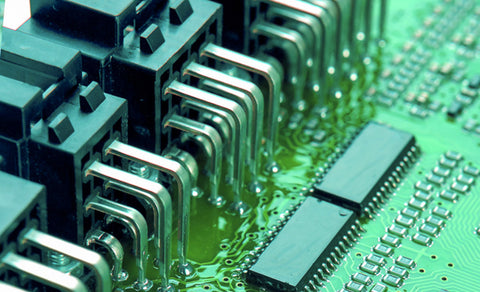
4. The lines are exquisite, the line diameter is required, and the size of the buried and through holes is appropriate.
Lines that can be made wide should not be made thin; high-voltage and high-frequency lines should be round and smooth, and there should be no sharp chamfers; no right angles should be used for corners. The ground wire should be as wide as possible, and it is best to use a large area of copper, which greatly improves the connection point problem. The wires are too thin, and there is no copper coating in the large unwiring area, which is easy to cause uneven corrosion.
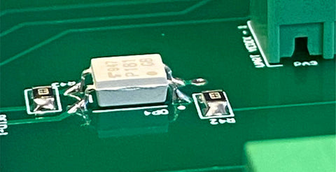
5. Pay attention to the number of vias, solder joints, and line density.
Although some problems occur in post-production, they are brought about by the satisfactory circuit board design. For example, if there are too many wire holes, the copper sinking process will bury hidden dangers. Therefore, the wire holes should be minimized in the design. The density of parallel lines in the same direction is too large, and it is easy to connect into one piece during welding; therefore, the line density should be determined according to the level of the welding process.