
Via is an integral part when comes to multilayer PCBs. These are used in PCBs to reduce the complexity of design, reduce impedance, increase connectivity and dissipate more heat. I said Vias are important don’t I? This article will serve as a guide to understand what is Via in PCB, how it is made? What are the types of Via and guide to use via your PCB design.
Via in PCB:
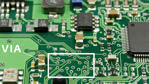
Simply put these are conductive copper cylinders that connects components, traces or planes from one layer of PCB to another layer. This provides the electrical and thermal connectivity between these layers. Each ends of the via uses a via pad to ensure connectivity. This is similar to copper pads we use for components and traces. In the above image you can see several Via placed on this layer of PCB it connects traces from this layer to other layers.
Importance of Via:
Usage of via in a complex PCB is extremely handy as it makes the design less complex. Imagine having over 20+ components to place in a PCB. The design can get really complex unless we provide connectivity within layers by using via. This will reduce the complexity as well as reduce the size of PCBs greatly.
Another key significance of Via is that it increase the connectivity between layers. It is a common practice for designers to place multiple via to connect a plane or track that carries high current from one layer to another. Typically this used for Ground or Power plane in PCBs. The multiple via will provide multiple conductive path for current to flow through and reduces the impedance for it. This will enable better heat dissipation and avoid malfunction.
This also applies to tracks which carries high speed signal where multiple via will reduce shorten the path of signal thus improving the functionality of the board.
Types of Via:
There are three types of Via which we can use in our PCB boards.
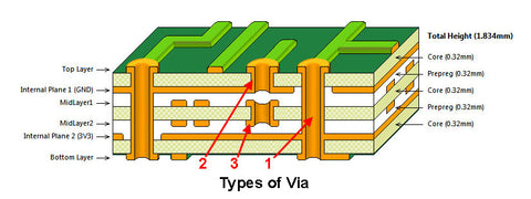
1. Through hole Via :
This is the most popular via to use in our PCB boards. This via connects one external layer to another external layer. Moreover this via is quite easy to implement for manufacturers as it involves drilling the board and uses chemicals to expose the copper within it . This provides the connectivity.
2. Blind Via:
These via are used in PCB with more than two layers. Suppose you are designing to a 4 layer PCB board, blind via can be used to connect top layer to 2nd or 3rd layer. These type of via requires manufacturer to pay special attention to placing this via rather than just drilling through the board.
3. Buried Via:
These are the via which connects only internal layers and will not be visible to user. For a 4 layer PCB board buried via will be used to connect layer 2 and 3. These type of via is less common in usage comparing to other two. Also it is recommended to avoid this type of via due to difficulty in implementing and troubleshooting issues that may occur.