
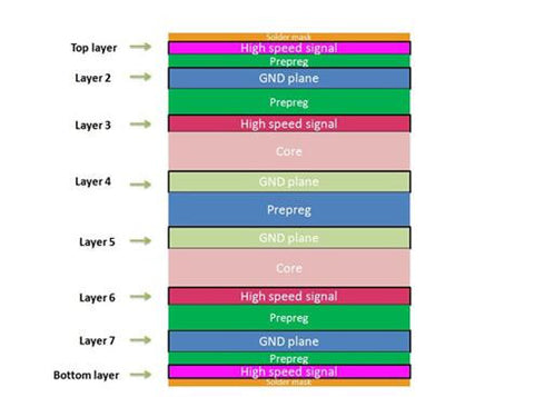
PCB layer stack-up, also called layer build-up, is the arrangement of insulating layers and conductive layers (copper layers) that make up the PCB before PCB layout design. Several insulating layers and copper layers are stacked together through the “prepreg” to generate a multiple-layered PCB. Here is an example layer stack-up of an 8-layer PCB.
Why need layer stack-up?
The demand for PCB layer stack-up is the result of the miniaturization, lightweight, and the multifunction of electronic products. The requirements for excellent performance and high reliability make multi-layered PCB popularity.
As the PCB densities and complexities are increased to adapt to the development of electronic products, the efficiency of la yer arrangement must be improved to avoid the problems such as cross talk, stray capacitance, noises, then achieve the purpose of improving the signal integrity.
The benefits of a well-designed layer stack-up
A poor-stacked PCB may increase the electromagnetic interference (EMI) and greatly lower the performance and reliability of the product. But a well-designed PCB layer stack-up help reduce the problems of signal cross talk and impedance mismatch on high-speed PCBs. And a useful stack-up will minimize the radiation and prevent the circuits from being interfered with by the outside noises. Besides, a well-stacked PCB provides better electromagnetic compatibility for your PCB design.
Some considerations and rules about PCB layer stack-up
1. The PCB structure should be designed based on the board size, circuit size, and EMC requirements.
2. The layer distribution should be symmetrical or balanced.
3. The thickness and the type of board materials are determined based on the characteristics of the materials, the thickness of the inner layer, the manufacturing process, etc.
4. Arrange the signal layer next to the internal power layer for tight coupling and avoid two signal layers is adjacent to each other.
5. The space between layers should be as small as possible to meet the requirement of miniaturization.
6. The copper weight, the position of the vias, and the vias types should be determined according to the specifications of your design.