
High density interconnects (HDI) layout refers to a set of techniques used to layout a PCB when traces widths generally drop below 8 mils (0.2 mm). These techniques are designed to ensure you can fit a higher density of components onto a single board, allowing you to keep your board size small while increasing component count. Not all boards need HDI layout techniques for a number of reasons, while some components require HDI techniques for proper routing.
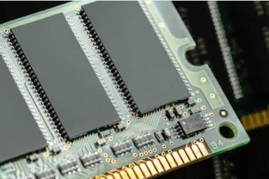
An HDI PCB board requires smaller vias to make layer transitions, particularly in fine-pitch BGA components and more traces per sq. mm. In order to accommodate fine-pitch components, you’ll find the following typical features in an HDI layout:
- Smaller vias: HDI PCB boards use microvias (mechanically or laser drilled), blind/buried, and staggered vias for layer transitions. These vias have smaller aspect ratios than typical through-hole vias. In order to use these vias with finer pitch components, their diameters are smaller, which then limits their useful depth.
- Thinner traces: The thinner traces used in HDI PCB boards are required to make connections to vias on each layer, as well as to in-pad vias. The thinner traces also allow higher trace density, thus the term HDI.
- Higher layer count: We’ve built non-HDI PCB boards with high layer counts, but HDI board layer counts can easily reach 20 or more layers when working with high pin density components (e.g., FPGAs).
- Lower signal levels: HDI boards are not used for high voltage or high current. This is because the high field strength between neighboring lines will cause ESD, and high currents will cause an excessive temperature rise in conductors.
If you look at the above points and the IPC standards, you can figure out when a board makes the transition to the HDI regime, thus requiring HDI layout and routing techniques. According to the IPC-2221A/IPC-2222 standards, the maximum recommended aspect ratio for through-hole vias is 8:1 (aspect ratio = via depth/via diameter). This means, for a standard thickness of 1.57 mm PCB, the minimum drill diameter for a through-hole via is 0.196 mm, or ~8 mils. If your vias need to be smaller to accommodate fine-pitch components, then you’ll need to use some HDI-specific via designs and thinner traces.