
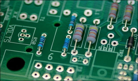
Through-hole assembly is a method for producing electronic circuits in which the components are installed through leads. It refers to the mounting process that inserts the leads to the drilled holes and solders the components on the board by wave soldering or manual soldering.
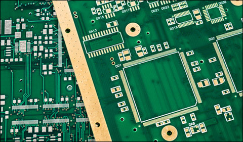
Over time, PCB design moved from single-sided boards to double-sided boards, then came the multi-layer boards. Through-hole assembly is difficult to meet the requirements of modern electronics. Nowadays, SMT technology has largely replaced through-hole construction in PCB manufacturing. But through-hole assembly is still irreplaceable in some applications, such as electrolytic capacitors, connectors, and large transformers.
The features of the through-hole assembly
· High reliability
The through-hole assembly provides higher environmental stress because the components are held on the board by using leads inserting into the holes rather than simply being soldered on the PCBs’ surface as the SMT components. Thus, through-hole assembly offers a more robust physical connection, making it the preferred process for the military and aerospace industry that have high-reliability requirements.
· Easy for manual operation
Through-hole components are easier to replace or adjust their position, making this assembly method widely used in the applications that need PCB testing and PCB prototyping.
· Higher durability
With high heat resistance and high-stress tolerance, through-hole components often appear in industrial machinery and equipment. Because through-hole LEDs are very bright and durable, you can find them in the LED lights on giant billboards.
· Lower manufacturing efficiency
Due to the extra step of drilling and hold the components using leads, through-hole assembly is time-consuming, which causes higher costs and lower production efficiency.
· Limited PCB design
Through-hole assembly is not suitable for multi-layer PCBs because drilled holes must cover all layers of the board, which increases the difficulty of layout design and PCB manufacturing. And the entire size of the board would also be bigger than SMT PCBs, causing their application area is more restricted.