
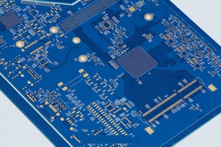
In PCB design, a solder mask layer is a negative plane and automatically generated on the top and bottom layers. That means, on the top and bottom layers, the visible shapes are PCB pads or holes, and the rest areas that are invisible should be printed or sprayed with solder masks in PCB manufacturing.
How is a solder mask formed? On a PCB, solder mask ink is printed or sprayed on the surface of the board and then baked or exposed under UV light. In this way, the ink dries and forms a protective coating, and this coating is the solder mask.
The solder mask permanently covers the surface of the circuit board and insulates the PCB externality from the outside environment.
Almost all PCBs require solder masks for protection and a longer lifespan. Only in some cases for better testing the design, PCBs without solder masks are needed, which are called naked PCBs. On rigid PCBs, the solder mask is also rigid. For flexible PCBs, flexible segments are added to the solder mask ink materials, and the solder mask called overlay is flexible.