
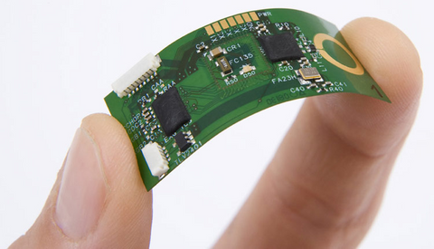
With the emergence of flexible PCB technology, modern electronic gadgets have come a long way. They are found in the core of many sensitive and delicate electronic products. Even your smartphone, camera, laptops, calculators, and many electronic gadgets are using this technology.
What is Flexible PCB?
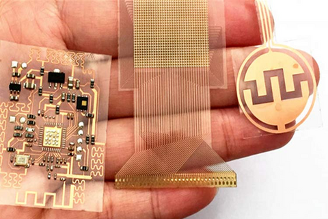
It is made of a base substrate material from polyimide. This material is found both naturally and synthetically and is used in various industries like automobile, clothing, etc. The compact nature of flexible circuits and high electrical-connection density offers us considerable weight, space, and savings compared to the traditional rigid printed circuit boards. This technology can reduce the total costs of electrical interconnections by up to 70% and wiring use by up to 75% when attached to the right application.
Moving forward, this article will guide you to a step-by-step manufacturing process of flexible circuit boards.
Step-by-step Manufacturing Process of Flex Circuit Boards
The manufacturing method is procedural and structured. Let’s understand three significant manufacturing steps:
STEP 1: Flex PCB Build Up
This is the primary phase, where the main focus is to save the base material. The primary material used for the flex circuit is polyimide. This material is expensive as compared to FR-4 and needs to be used properly. For appropriate polyimide usage, you need to keep circuits close to each other as much as possible using the nesting technique. The prototype PCB manufacturing includes the following processes:
Looping: Adding a slight amount of extra material beyond the designer's limit is acceptable. This extra material is known as a service loop that enables the servicing length and circuit assembly.
Sizing conductor: It provides the greatest flexibility, thus you need to select the thinnest copper, particularly when you want to use the circuit for dynamic applications.
Etching: This process is done to compensate for any isotropic losses in the manufacturing process. During this process, the line width loss is almost twice the copper foil thickness. Several factors impact the line width, like different types of copper, etch mask, conductor, etc.
Routing: Routing of the conductors can be done easily. Simply get on the perpendicular position to the bend and fold. This will improve folding and bending by reducing stress.
Ground Planes: Create ground areas crosshatched if the electrical allocation is adequate. This aids in improving the flexibility of the circuit by reducing the weight of the circuit board.
STEP 2: Flexible Printed Circuit Board (PCB) Fabrication Process
Now, let’s focus on the boards. It starts with conductor spacing and width. Polymer thin films require a standard conductor width, i.e. 375 micrometers. Simultaneously, the nominal polymer thick films and silver-based polymer films carry the desired percentage of circuit current. The diameters of holes in flexible PCBs can vary depending on the design and application.
Size of the holes: The manufacturer can create small holes and is also capable of a flexible PCB layout to be well inclined. With advanced technology, you can make holes as small as possible (i.e. 25 μm).
Filleting: Filleting is a technique where you can multiply the area of the pad and divide the stress. All the pads and land termination points on your flexible circuits need filleting. Plated through-holes is appropriate to create a reliable solder joint.
Button plating: Here, you can create a substitute plated through-hole. These days, manufacturers use copper to prepare vias and through-holes.
STEP 3: Concentrate On Physical Constraints
In this process, manufacturers deal with cover layers and cover coating problems. We bring to you a few common cover layers used in the process:
Adhesive-backed films: It is appropriate for dynamic flex circuit apps as it consists of raw materials. Adhesive-backed films are used mostly for over-coating custom PCB.
Screen-printable liquid overcoats: Screen-printable liquid overcoats are pocket-friendly and are generally used with thick polymer films.
Photo imaginable liquid and film polymers: It is the most advanced method of over-coating and has some surprising functionalities like:
- It acts as a solder mask and prevents the solder from circuiting traces.
- It protects the printed circuits from both external and internal damages.
- It prevents circuits from external electrification.