
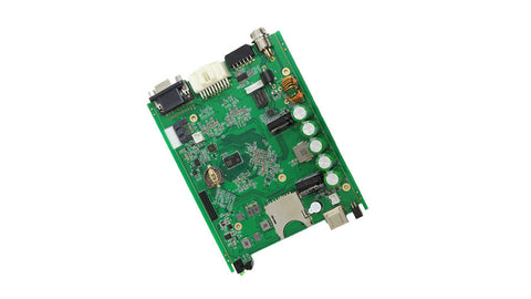
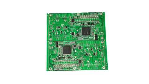
The screen printing layer of the PCB board is the text layer. Its function is to facilitate the installation and maintenance of the circuit, and print the required logo patterns and text codes on the upper and lower surfaces of the high density pcb, such as component labels and nominal values, component shapes and manufacturer logos, production dates, etc. So what are the specifications and requirements of basic pcb screen printing? How to add PCB screen printing?
The screen printing layer is the text layer, which belongs to the top layer of the electronic printed circuit board and is generally used for marking. The correct character layout principle of the screen printing layer is: “no ambiguity, no stitches, beautiful appearance”. This is to facilitate the installation and maintenance of the circuit, and print the required marks and special layers of character coding on the upper and lower surfaces of the printing plate.
1. All parts, mounting holes and positioning holes have corresponding silk screen labels. In order to facilitate the installation of the board, all components, installation holes, and positioning holes have corresponding silk-screen labels. The mounting holes on the electronic circuit are silk screened H1 and Hn. next identification.
2. The silkscreen characters are displayed in the order from left to right and bottom to top. For polar devices, such as electrolytic capacitors and diodes, make sure the orientation of each functional unit is the same.
3. There is no silk screen on the tin pad or the tin bath to be lined with tin, and the position number of the equipment should not be blocked by the equipment after installation. (High density, except smt circuit board without screen printing)
4. In order to ensure the welding reliability of the equipment, it is required that there is no screen printing on the pads of the equipment. In order to ensure the continuity of the tin lining, it is required that the tin lining has no silk screen; in order to facilitate the installation and maintenance of the equipment, the position number after the equipment is installed should not be blocked by the equipment. Do not press on the through holes and pads during silk screen printing, so as not to open and block the welding window and cause some screen printing loss, which will affect the training. The screen spacing is greater than 5mil.
5. The polarity of polar components is clearly indicated on the silk screen, and the polarity direction mark is easy to identify.
6. The number of sheets of the fr4 pcb board light-painting file is correct, each layer should have the correct output, and the complete number of layers should be output.
7. The identifier of the device on the quick pcb fabrication must be consistent with the identifier in the BOM list.
8. The direction of the directional connector is clearly indicated on the silk screen.
9. There should be a barcode position mark on the small batch pcb. If the space of the PCB board allows, there should be a 42*6 barcode screen printing frame on the black pcb board, and the position of the barcode should be considered for easy scanning.
10. The screen printing position of the board information such as circuit printed board name, date, version number, etc. should be clear. The printed board information such as board name, date, version number, etc. should be printed on the PCB file, and the location is clear.
11. There must be complete relevant information of the manufacturer and anti-static label on the PCE.