
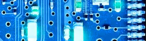
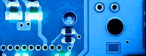
The common detection methods of PCB Circuit boards in the production process are as follows:
1. Manual visual inspection of 94v0 PCB board
Using a magnifying glass or calibrated microscope, operator visual inspection to determine if a circuit board is out of order and to determine when corrective action is required is the most traditional inspection method. Its main advantages are low upfront cost and no test fixtures, while its main disadvantages are human subjective error, high long-term cost, discontinuous defect discovery, difficulty in data collection, etc. At present, this method is becoming less and less feasible due to the increase in PCB production and the shrinking of the wire spacing and component volume on the PCB.
2. High level circuit boards online test
Through the inspection of electrical performance to find manufacturing defects and test analog, digital and mixed-signal components to ensure that they meet specifications, there are several test methods such as bed of needles tester and flying probe tester. The main advantages are low cost of testing per board, strong digital and functional test capabilities, fast and thorough short and open testing, programmable firmware, high defect coverage and ease of programming, etc. The main disadvantage is that it requires testing fixtures, programming and debugging time, high cost of making fixtures, and difficulty in use.
3. Printed circuit boards function test
Functional system testing is to use special testing equipment in the middle and end of the production line to comprehensively test the functional modules of the circuit board to confirm the quality of the circuit board. Functional testing can be said to be the earliest automated testing principle, which is based on a specific board or specific unit and can be done with a variety of devices. There are types such as final product testing, state-of-the-art mockups, and stacked testing. Functional testing usually does not provide in-depth data such as foot-level and component-level diagnostics for process improvement, and requires specialized equipment and specially designed test procedures. Writing functional test procedures is complicated, so it is not suitable for most circuit board production lines.
4. Automatic optical inspection
Also known as automatic visual inspection, it is based on optical principles and comprehensively adopts various technologies such as image analysis, computer and automatic control to detect and process defects encountered in production. It is a relatively new method for confirming manufacturing defects. AOI is usually used before and after reflow and before electrical testing to improve the pass rate of electrical processing or functional testing. At this time, the cost of correcting defects is much lower than the cost of final testing, often up to ten times.
5. Automatic X-ray inspection
Using the difference in the absorption rate of X-rays by different substances, see through the parts that need to be inspected and find defects. It is mainly used to detect ultra-fine pitch and ultra-high density circuit boards and defects such as bridging, chip loss, and misalignment generated during the assembly process. It can also use its tomography technology to detect internal defects in IC chips. It is currently the only way to test BGA soldering quality and shadowed solder balls. The main advantage is the ability to inspect BGA soldering quality and embedded components, no fixture cost; the main disadvantage is slow speed, high failure rate, difficulty in inspecting reworked solder joints, high cost, and long program development time, which is a newer inspection. method, remains to be further studied.
6. Laser detection system
It is the latest development in PCB testing technology. It scans the printed board with a laser beam, collects all measurement data, and compares the actual measurement to preset acceptance limits. This technique has been proven on bare boards and is being considered for assembly board testing at a speed sufficient for mass production lines. Fast output, no fixture required, and visually unobstructed access are its main advantages; high initial cost, maintenance and usage issues are its main disadvantages.
7. Size detection
Use the two-dimensional image measuring instrument to measure the hole position, length and width, position and other dimensions. Since the soldering pcb board is a small, thin and soft type of product, it is easy to deform in contact measurement, resulting in inaccurate measurement. The two-dimensional image measuring instrument has become the best high-precision dimensional measuring instrument. After being programmed, Sirui’s image measuring instrument can realize fully automatic measurement, which not only has high measurement accuracy, but also greatly shortens measurement time and improves measurement efficiency.