
Different Types of Vias in PCB
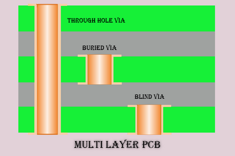
In a printed circuit board (PCB), via is a simple copper plated hole that connects one layer to another layer. In a generic double-sided PCB, via connects the top layer to the bottom layer, which is called through-hole vias. Vias are just drilled holes that are plated with copper in a PCB, and due to advancement in technology and precision machinery, we can drill vias that do not penetrate the surface but only got halfway through, these are called blind Via. There exists another type of via that can only exist in multi-layer PCBs. This via is sandwiched in between two or more copper layers, those are called buried vias. as you can see in the above image.
So in this article, we will take a look at different types of vias and understand how can we implement them in a practical design to improve component density in a PCB. In many of the previous projects, we have to utilize PCBs in order to improve the stability and efficiency of the circuit, you can check those out if you are interested. You can also check out our article on the basics of PCB if you are new to PCB making industry.
What is a Via?
As you can see in the image, vias are copper-plated holes that connect one layer to another in a standard two-layer PCB. This is done by first drilling a hole, and then electroplating the drilled hole using electrolysis. The standard via is called a through-hole via, but there are some major drawbacks of through-hole vias in surface mount technology. If the requirement is a high-density board, then this via occupy more space and it affects the overall density of the board to solve this problem. PCB design-engineers use a blind via or a buried via instead. In this section, we will talk about all that in detail.
What is a Blind and Buried Via?
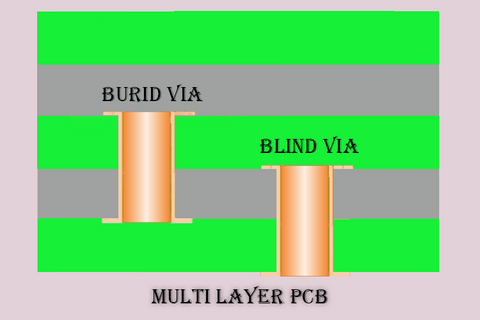
In the case of a blind via, the via connects one of the external layers (that can be the top or the bottom layer) to an inner layer of the PCB.
In the case of buried via, it connects only two inner layers and the via is buried in between the top and bottom layer and in case of multi-layer PCB, this via can be buried inside several layers, that is why it is called a buried via
Blind and buried vias are used in High-Density Interconnection (HDI) boards because they optimize the density of the board by placing components close together.
What are Stacked and Micro via?
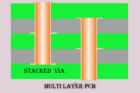
Stacked vias are cleverly laminated vias they can be blind and buried vias. These types of vias connect multiple layers on a PCB that is why it is named stacked via. Generally, in PCB, they are connected in such a manner that they appear to be looking in a sideways direction. This via looks like vias are on top of each other.
As the name implies micro via is a very small via. It is so small that you cannot see it without a microscope. Micro vias are often used in high-density PCB because the smaller the diameter, the more routing space you have on your board, and micro vias also reduce parasitic resistance and capacitance, which is a typical part of high-speed circuit design. However, one major drawback of micro via is that it requires more drilling time and there is a high chance the drilled hole can get off-center.