
With the development of electronic technology, many electronic products are developing in the direction of miniaturization and precision, and the requirements for SMT chip processing will become higher and higher. Welding requirements and conventional welding process, the welding of components, the main attention is: master the heating time, use the appropriate temperature and good operation.
Welding of different components, in different temperature, air flow and other environments, using different electric soldering irons and soldering iron tips, the skills to be mastered in these three aspects are also different, which requires us to get exercise in a lot of practical operations and improve.
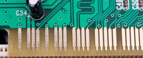
For example, the welding requirements of 0201 SMT components are generally higher than those of 0402. Ensuring the quality of chip welding is one of the processing requirements of electronic processing plants. The quality of solder joints is the core of SMT chip processing. The quality of solder joints is directly related to the quality of this PCBA. So how should the quality of solder joints be detected?
1. Appearance inspection:
1. There can be no missing components;
2. There can be no component paste errors;
3. There can be no short circuit phenomenon;
4. There can be no virtual welding phenomenon.
2. External performance:
1. Good wettability, the edge of the welding point should be thin;
2. The surface of SMT solder joints with good quality is complete and smooth and bright;
3. The appropriate amount of solder and the solder completely cover the soldering parts of the pads and leads, and the height of the components is moderate.
3. Judgment of virtual welding:
1. Visual or AOI inspection.
2. Use special equipment for online tester for inspection.
Fourth, the cause and solution of virtual welding:
1. For PCBs that have been printed with solder paste, the solder paste is scratched and rubbed, which reduces the amount of solder paste on the relevant pads and makes the solder insufficient. should be replenished in time.
2. The pad design is defective. The presence of through-holes in the pads is a major defect in circuit board design. Generally, it is not recommended to use them. Through-holes will lead to the loss of solder during SMT chip processing and cause insufficient solder.
3. The PCB board has oxidation phenomenon, that is, the pad is black and not bright, and the oxidation phenomenon can be removed by an eraser. Generally, when the PCB is damp, the small batch processing factory of SMT proofing is placed in a drying oven for drying. If there are oil stains, sweat stains and other contamination on the board, clean it with absolute ethanol.