
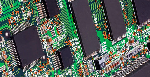
What is a double-sided pcb board?
Double-sided boards have wires on both sides, but if wires are to be used on both sides, there must be a proper circuit connection between them. The “bridges” between these circuits are called vias. A via is a small metal-coated hole in a circuit board that allows wires to be connected from both sides.
Since the area of the double-sided board is twice that of the single-sided board, the double-sided board solves the difficulty of staggered wiring on the single-sided board, and the simple circuit board is also more complicated than the single-sided board.
What is a multilayer circuit board?
In order to increase the wiring area, multi-layer boards mostly use single-sided or double-sided wiring boards. It is a smd prototype board with one inner layer and two outer layers, or two inner layers and two outer layers.
The printed circuit board has interconnected conductive patterns, and the combined materials are used alternately, and the conductive patterns are connected to each other according to the design requirements to become a 4 layer pcb fabrication or six-layer printed circuit board, also known as a “multi-layer printed circuit board”.
The number of layers on the board does not imply that there are multiple independent routing layers. In special cases, a blank layer is added to control the thickness of the board. Usually the number of layers is an even number, and most motherboards have the outermost two layers. The side layers are 4 to 8 layers. Due to the dense number of PCB layers, it is usually not easy to determine the actual number of layers, but it can still be judged by careful observation of the motherboard.
The main difference between a multilayer board and a double-sided board is the addition of internal power and ground planes. Power and ground nets primarily use the power plane.
The wiring of the multi-layer board is mainly the upper and lower layers. Supplementing the middle wiring layer, the design of the multilayer board is basically the same as the design method on both sides. The key is how to optimize the wiring of the internal electrical layers to make the wiring of the circuit board more reasonable.