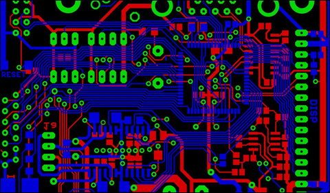
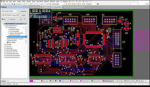
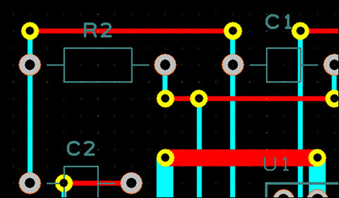
A printed circuit board (PCB) design is not an easy thing. It is a critical part of the design of electronics product and includes PCB routing and component placement layout. The performance of the circuit will largely depend on its layout on the PCB, so it is important to learn more about the PCB design & layout techniques.

The PCB design and layout steps in Altium Designer
To create a good PCB layout design, engineers need a suitable PCB design software to layout the circuits. There are several kinds of PCB design software that are preferred by PCB engineers or students: Eagle, Altium Designer, Protel, OrCAD, EasyEDA, KiCAD, etc. Altium Designer is a popular PCB design software. We take the Altium Designer as an example to list the design steps:
Create the schematics
Create a blank PCB layout
Capture the schematic and link to the PCB
Design the PCB stack-up
Define the design rules and DFM requirements
Place components
Insert the drill holes
Route traces
Add labels and identifiers
Generate design files

Professional engineers know that suitable design software is essential for PCB design. How to choose a PCB design software according to your actual situation? First, you should consider whether the software can meet your needs. Second, if the design software is easy to use or not. And you also need to know if the design software works best in making single-layer design or multi-layer PCB layout.
Some tips in PCB layout design
There are some PCB design tips for improving the practicability PCB layout design and reduce unnecessary troubles.
Overall PCB layout
It is best to draw an initial plan for the significant components and circuits when starting a PCB design, which is facilitated to decide the board area and the numbers of track layers.
Copper traces
Copper traces should be neat and smooth. And you will find that most of the copper traces on PCB bend at 45° angles in professional PCB designs. The reason is that 45° angles shorten the electrical path between components when compared to 90° angles. And for the high-speed circuits, it is best to avoid 90° angles.
Ground cables and power cables
Some critical copper cables like ground and power cable should be as thick as possible to improve the anti-interference ability and power efficiency.
 、
、
Partition design
The circuit can be divided into several parts without affecting the circuit performance. This kind of PCB layout not only helps to reduce mutual interference but also makes the circuits appear clean and orderly, which is convenient for checking and maintenance in the future.
It should be noted that engineers should follow the guidelines of the PCB layout to meet the manufacturing requirements and safety standards. A professional PCB layout design helps control the manufacturing cost and improve the performance of the products in a limited space. If you need more details about the PCB layout design or PCB manufacturing, please contact us.
