
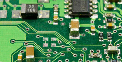
PCB Splicing not only involves the quality of the PCB board, but also affects the cost of PCB production. How to make a reasonable and effective boarding under the premise of ensuring the quality of PCB circuit boards is a problem that PCB engineers and PCB manufacturers pay great attention to.
How to make a reasonable and effective PCB Splicing?
1. The width of fr4 circuit board is ≤260mm (SIEMENS line) or ≤300mm (FUJI line); if automatic glue dispensing is required, the width of the PCB board × length is ≤125 mm×180 mm.
2. The shape of the blank circuit board should be as close as possible to the conventional graphics. It is recommended to use 2*5 and 3*3 panels, which can be determined according to the thickness of the board.
3. The outer frame of the quick turn pcb should adopt a closed-loop design to ensure that the jigsaw board will not be deformed when fixed on the fixture.
4. The center distance between pcba boards is controlled between 75 mm and 145 mm.
5. There should be no large components near the connection points between the shape of the jigsaw puzzle and the small board inside the custom pcb boards, between the small board and the small board, and there should be more than 0.5mm of space between the components and the board edge.
6. Four positioning holes are made at the four corners of the outer frame of the pcb puzzle board, plus Mark points, with a hole diameter of 4mm (±0.01mm); the strength of the holes should be moderate to ensure that they will not break during the upper and lower boards, and the hole walls are smooth and without glitch.
7. In principle, the QFP with a spacing of less than 0.65mm should be set at its diagonal position; the positioning reference symbols used for the imposition PCB sub-boards should be used in pairs and arranged at the opposite corners of the positioning elements.
8. When setting the reference positioning point, usually leave a non-resistance area 1.5 mm larger than it around the positioning point.
9. Large components in bare printed circuit board should have positioning posts or positioning holes, such as I/O interface, microphone, battery interface, micro switch, headphone interface, etc.