
Mainly for board-on-board contacts, plated half-holes PCBs or castellated holes are used, often when two printed circuit boards are mixed with various technology. For example, the configuration of complex modules of microcontrollers and typical individual PCBs.
Further implementations are displays, HF, or concrete modules soldered to the base circuit board.
Therefore, board-on-board PCBs require plated halves that act as SMD attachment pads. By linking the PCBs directly together, it is significantly thinner than a similar link with multi-pin attachments.
We may also illustrate it like this,
High density and multifunction, and mechanization became a standard in the future for the exponential growth of electronic devices. The board components develop in geometric indexes, but the PCB sizes are increasingly smaller, so they must relate to the supporting board. As the round hole is poured with soldering flow into the motherboard, a cold solder will be generated that will cause the board and the motherboard to have a weak electrical link since the round hole volume is high because there is a plated PCB half hole.
CASTELLATED HOLE FABRICATION PROCESS:
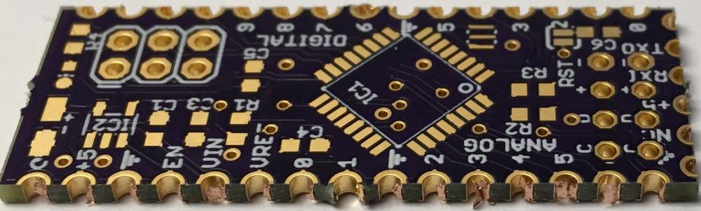
- Drilling – boiling – picture conversion – pattern boiling – striping – etching – floor layer – surface covering – half holes plating.
- Since plated half-holes PCB is used to mount one PCB immediately on top of another PCB, two conditions are:
- It requires electric contacts, not just external connections;
- The range between the two boards is gap or none.
The half-holes plated are cost-effective linking strategies that transform the circuit board into sub-assembly on the wall. They are typically mainly in fine-pitch SMD or on portable radios or RF assemblies. The panels will provide a perfect soldering landing since they are concave and plated. They are at the borders of the PCB stands for the motherboard or mounting surface pieces flush into the motherboard surface. The only suit would there be no space for air or dust to collect.
SPECIFICATIONS OF PLATED HALF HOLE:
The printed circuit board has several specifications, but the critical thing that you will use with a PCB is,
- Half hole printed circuit board
- High quality and cost-effectiveness
- OEM and ODM PCBs are accessible
- certified ISO9001, UL, RoHS
APPLICATION OF CASTELLATED HOLE:
Plated half-hole boards are used for the telecommunications, computing, automotive, gas, car, and high-end technology sector, and so on.
ADVANCED AND STANDARD HALF HOLE PCB FABRICATION:
Both bare PCB and advanced PCB are equipped with plated half holes. The sample required of castellated holes is 0,6 mm for the standard PCB service. The actual size between two half-hole plates is 0.55 mm. Only experts will give you the highest-quality PCB with the highest quality plates that suit the requirements and adhere to the strictest specifications of PCB manufacturing and assembly.
WHY USE HALF HOLE EXPERTISE IN PCBs?
We never glance up when it comes to innovation. Sometimes the outdated technology doesn’t seem to go down. One example is the plated PCB castellated holes installation technology for the electronic components, which appears to be hung today, mainly through modern designs that need specific functions.
But is it that easy? Why use half-hole technology on printed circuit boards when the technology components on the surface mount seem smaller and facilitate compacter positioning on the PCB? As with other design choices, the use of each component form involves compromise. Let us begin with a quick rundown of the plated half-hole installation technology and surface mount technology related to the PCB design phase of the printed circuit board.
PASSIVE HALF-HOLE TECHNOLOGY:
Two possible forms of sets, radial and axial, have passive half-hole modules. A longitudinal direction component with a half-hole has its electrical conduits around the reciprocating air of the object. Think of a simple capacitance; the electrical pipes are running around the cylindrical resistance axis. Diodes, inducers, and even condensers are equally installed. Not all halved components are cylindrical; some elements, such as high-power resistors, are available in rectangular bundles with reliability is important which runs down the product width.
In the meantime, radial parts have electrical conduits that stand out from one end of the piece. Many oversized electrolytic condensers are packed in this manner, enabling them to be placed on a board with a hole pad and take up a smaller room on the circuit board. Others devices are packaged as radial half-hole components, such as switches, LEDs, short relays, and fuses.
ACTIVE PLATED HALF HOLE:
If you recall your electronics lessons now, you would also remember the embedded DIP or acrylic DIP circuits that you had (PDIP). These modules are usually considered to be installed on proof-of-concept breadboards but are generally found in actual PCBs. The DIP kit is standard for organic compounds, such as op-amp bundles, low voltage controls, and many other similar components. Other parts such as transistors, higher voltage regulators, quartz resonators, higher power LEDs, and several others may be supplied in a zigzag inline (ZIP) or transistor contour (TO) kit. Like axial or radial passive half-hole technology, these other packages are often mounted onto a PCB.
Plated half-holes came when manufacturers were more worried about the mechanical stability of electrical devices and less concerned about esthetics and signal accuracy. The emphasis was less on space reduction in the modules and no issue with signal integrity. Later on, as the central stage started to be played by power usage, signal integrity, and board room, designers wanted components of the same electrical versatility in a smaller box. This is where elements of the surface mount fall in.
SURFACE SUPPORT TECHNOLOGY:
You would probably see boards controlled by surface mounting modules if you look at some recent half-hole PCB style. Newer architectures also use half-holes, although these modules are most commonly found in electronics and other heat-producing applications. Surface mounting technology is today the most widely applied packaging component technology. This part of the form does not use electrical pins. The leads instead appear as tiny metal pads along the same side of the region. The primary aim of these pads is that the layer of a PCB may be soldered specifically during installation.
The usage of surface mounting pads relative to half-hole technology offers some benefits, as described below. The smaller pad size and the overall component size both lead to the less visible parasite of these components. This enables them to be run at higher speeds or rates until you notice issues with signal integrity.
You probably recall the Pentium processors with a range of buttons on the bottom of the device when you recall your old PC. This product form is a Pin Grid Array (PGA), equivalent to the more advanced LGA package. A PGA component can appear to be a half-hole module, but it does not solder through board holes. Instead, it plugs the soldiers into a surface-assembled box onto the floor. This makes it easy to replace or update the PGA part if required.
COSTS DIFFERENCE BETWEEN TWO TECHNOLOGIES:

The components in the surface mount appear to be smaller than the half-hole counterpart. It does not always suggest that the cost of the surface mounting part is often lower merely because the manufacture of the components requires fewer raw materials. Surface mounting components themselves may cost the exact price as a hollow part equivalent. However, after automatic assembly costs per part have been taken into account, the average cost per surface assembly component is generally lower than a complete component with almost the same cost function, power or voltage, and acceptance criteria.
This disparity is caused by the need to position through-hole components in the PCB, which cause task-oriented. In comparison, surface mounting elements, which account for the cost differential, do not include drilling. The issue arises: if the mounting components of the surface are smaller, more accessible, and cheaper. The solution depends on the application case for the configuration of your PCB. Yes, PCB technology is ancient, extensive, and costly, but there are advantages.
PROS AND CONS OF HALF HOLE PCBs:
Even if half-hole PCB has been used by the experts but has several advantages and drawbacks before we agreed to use them, we must know both the advantages and disadvantages of half-hole PCBs.
PROS:
- Easier to use prototypes
- Huge defensive links
- Resistance to heat
- Capacity to handle power
CONS:
- Increased board costs due to boiling
- Occupies more real estate board
- PCB assembly involves more
- Higher velocities
The parasite in half-hole PCBs and the parasite produced in the PCB structure are a problem for cars, aerospace, and military goods that must be highly robust but must also operate well into GHz belts. A half-holder PCB can lead to increased input impedance along with interconnection at mm-wave frequencies. There are several issues. However, in these applications, PCB half-hole is preferred, so solder levels are less prone to malfunction during service. In this place, there is still plenty of creativity.
Technology leaders often move into a linked community, and when it comes to PCB architecture, scale matters. In the quest toward all-around computation, IoT, or “environmental intelligence,” we all want the board itself to be the drive to create smaller and smaller modules. Smaller components enable smaller boards that allow us to make printed circuit boards in almost any form. Smaller sizes entail lower costs of production. Less costly modules and panels provide the end-user with cost reductions.
Half-hole mounting technology is ideal for prototyping and experimenting since you can switch parts quickly on a printed circuit board. And before you build your board, you may add half-hole technology to your design.