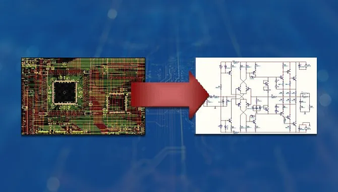
• Different Internal Structures
A passive crystal oscillator consists of a quartz crystal, electrodes, and a ceramic base.
An active crystal oscillator, on the other hand, adds an IC (Integrated Circuit) on top of the passive crystal oscillator, which is an independent oscillation starting chip.
• Different Crystal Oscillator Casings
If there is a dot (·) in the lower-left corner of the crystal oscillator casing, it is an active crystal oscillator. The dot (·) represents the position of pin 1, which is often defined as the tri-state* in clock oscillators. Passive crystal oscillators do not have a dot (·) marking on their casings.
*Tri-state: The output can be either the normal high ("1") or low ("0") logic levels found in typical binary logic circuits, or it can remain in a high-impedance state (Hi-Z).
• Different Pin Configurations
A passive crystal oscillator does not require a power supply connection and can operate with various voltages. Therefore, it typically has only input and output pins. It relies on an external clock circuit (connected to the internal oscillator circuit of the main IC) to generate the oscillation signal as it cannot oscillate on its own. The following diagram shows the pin assignment for a passive crystal oscillator.
An active crystal oscillator requires a dedicated power supply and typically has four pins: one pin left unconnected, the second pin connected to ground, the third pin serving as the output, and the fourth pin connected to voltage. It can operate without the need for external matching capacitors. The following diagram shows the pin assignment for an active crystal oscillator.
]]>VCC is used as the positive supply voltage for circuits using a bipolar transistor (BJT).
The positive supply voltage on the collector side of the NPN bipolar transistor is "VCC". The collector terminal of an NPN bipolar transistor is often connected directly to VCC or VCC through a resistor or other means.
The "C" in "VCC" stands for Collector. It is widely believed that the reason for repeating "VCC" and "C" twice is to distinguish it from the collector voltage VC.
Circuits that use multiple positive supply voltages are often represented by different supply voltages, such as "VCC1, VCC2, …".
VCC is also used as the positive supply voltage for operational amplifiers, whose main elements that make up the internal circuit are bipolar transistors, and for TLL (Transistor-transistor logic).
Supplement
"V+" and "V-" also represent the power supply voltage.
Therefore, "V+" may be used instead of "VCC" for the positive supply voltage of circuits using a bipolar transistor (BJT).
VEE is used as a negative supply voltage for circuits that use a bipolar transistor (BJT).
The negative supply voltage on the emitter side of the NPN bipolar transistor is "VEE". The emitter terminal of an NPN bipolar transistor is often connected directly to VEE or VEE through a resistor or other means. In the case of a single power supply system, "VEE" is at the same potential as the ground.
The "E" in "VEE" stands for Emitter. It is widely believed that the reason for repeating "VEE" and "E" twice is to distinguish it from the emitter voltage VE.
Circuits that use multiple negative supply voltages are often represented by different supply voltages, such as "VEE1, VEE2, …".
VEE is also used as the negative supply voltage for operational amplifiers, whose main elements that make up the internal circuit are bipolar transistors, and for TLL (Transistor-transistor logic).
Supplement
"V+" and "V-" also represent the power supply voltage.
Therefore, "V-" may be used instead of "VEE" for the negative supply voltage of circuits using a bipolar transistor (BJT).
VDD is used as the positive supply voltage for circuits that use a field-effect transistor (FET).
The positive supply voltage on the drain side of the N-channel field-effect transistor (NchFET) is "VDD". The drain terminal of an N-channel field-effect transistor (NchFET) is often connected directly to VDD or VDD through a resistor or other means.
The "D" in "VDD" stands for Drain. It is widely believed that the reason for repeating "VDD" and "D" twice is to distinguish it from the drain voltage VD.
Circuits that use multiple positive supply voltages are often represented by different supply voltages, such as "VDD1, VDD2, …".
VDD is also used as the positive supply voltage for operational amplifiers, whose main elements that make up the internal circuit are field-effect transistors, and for CMOS(Complementary MOS).
Supplement
"V+" and "V-" also represent the power supply voltage.
Therefore, "V+" may be used instead of "VDD" for the positive supply voltage of circuits using a field-effect transistor (FET).
VSS is used as the negative supply voltage for circuits that use a field-effect transistor (FET).
The negative supply voltage on the source side of the N-channel field-effect transistor (NchFET) is "VSS". The source terminal of an N-channel field-effect transistor (NchFET) is often connected directly to VSS or VSS through a resistor or other means. In the case of a single power supply system, "VSS" is at the same potential as the ground.
The "S" in "VSS" stands for Source. It is widely believed that the reason for repeating "VSS" and "S" twice is to distinguish it from the source voltage VS.
Circuits that use multiple negative supply voltages are often represented by different supply voltages, such as "VSS1, VSS2, …".
VSS is also used as the negative supply voltage for operational amplifiers, whose main elements that make up the internal circuit are field-effect transistors, and for CMOS(Complementary MOS).
Supplement
"V+" and "V-" also represent the power supply voltage.
Therefore, "V-" may be used instead of "VSS" for the negative supply voltage of circuits using a field-effect transistor (FET).
Help is at hand. There are many suppliers on ebay that will sell you a small TFT already mated to a PCB with the FPC connector broken out into a 2.54mm DIP header. If these satisfy your needs then buy them, you’ll be saving yourself a whole lot of work.
But what if the panel you want only comes ‘naked’, or perhaps you want to drive the signals directly as you’ll have to do if you want to stream video to it. If you fall into these categories then you are going to have to tackle the FPC connector yourself, and I’m going to show you how.
The breakout board is suitable for many different FPC pin pitches. By holding the FPC connector up against the board I can see that mine has a 0.8mm pitch and 37 terminals. As a bonus I can see that each terminal has a very small hole punched in it. This hole is designed to allow solder to flow up from underneath, making a better connection.
We are going to use a reflow technique to solder this connector. The idea is that we lay down solder on to the board pads and then reflow it to create the connection. I was surprised how easy this was.
Make yourself a spatula from some folded paper and use it to spread flux as evenly as you can across all the pads that you’re going to use.
You can do this with a standard size soldering bit since we’re going to be using the side of the bit, not the tip. However I’m going to fit my 1mm bit and use that because I’m going to need it later and I don’t want to change it.
Melt a decent blob of solder on to your iron and hold it such that the side of the bit will come into contact with the pads. Now drag your iron across all the pads in an even motion that should take about 3 seconds to go from side to side.
The trick here is that the solder is attracted to the pads and repelled by the board in between. Examine the results and if any of the pads have been missed then drag the iron over again until you’re happy.
Use your magnifier or microscope to inspect for solder bridges between pads. If there are any then wick up the solder bridge. There were no solder bridges when I did it so I did not need to do any remedial wicking.
Now clean up the flux with some Isopropyl Alcohol (IPA). IPA is cheaply available in small bottles sold as camera lens cleaning fluid.
I need to mask off the traces on the board that I’m not going to use so that they won’t create short-circuits during operation. I use electrical insulation tape to do that.
Masked off pads
Fully masked.
This adaptor board has traces on the flip side that need to be masked off.
The flip side.
The last thing to get the masking treatment is the aluminium underside of the TFT panel.
Now is a great time to solder the DIP header into place because you’re not going to be able to get to it easily after the FPC connector has been soldered down.
You can either buy a DIP header that suits your size requirements or you can cement your reputation as a backroom hacker by cutting a pair of SIP headers to size and supergluing them together to make a DIP! No prizes for guessing what I did…
Now the fun part. This need not be difficult and you can greatly increase your chances of success by preparing well.
You are going to need to do this under a microscope or powerful magnifier. The microscope will have built-in illumination, if you are working with a magnifier then ensure that you have your work area under a bright light.
We need to find a way of totally eliminating the natural shaking that the human body will transmit through the soldering iron, and do so with 100% repeatability as you work on each terminal. Here’s how.
Find a metal bar that you can use to rest the hot part of the iron on without setting fire to anything. With the hot part of the iron resting on the bar practice pivoting the iron over it so that the bit can be brought down on to each terminal. This method completely eliminates your body’s natural shake allowing you to work as accurately as if you were a robot. Believe me, my preparation for this operation consisted of a night-before of beer and curry followed by three cups of fully caffeinated black tea in the morning right before I started this and I had a 100% success rate using this technique.
Before starting on the FPC connector make sure you paste a thin layer of flux over the tinned board connectors. This will help the solder to reflow smoothly over the FPC terminals.
Working under the microscope or magnifier, carefully align the FPC connector with the tinned pads ensuring that it’s straight and that each terminal is completely overlapping the pad. Don’t overlap the pad more than the terminal length because there may be some traces further back on the connector that could cause a short circuit. Hold it down like that with one of your hands.
Now with your soldering iron in the other hand with a clean bit with no solder on it pivot over your metal bar until you are pressing down on the first terminal. The solder below the terminal will melt and bubble up through the tiny hole in the terminal. Lift the iron and let it set. Do the same for the terminal at the other end of the connector.
Now you can just repeat the process for every pin along the connector. When you’re done go back and check each terminal, repeating the pressing down with the iron process for any terminal that is still sitting up above the board – there will always be one or two like this.
The terminals that you have just soldered are quite delicate and if allowed to flex then they can easily snap off. Our final step then is to tape down the joint so it cannot flex and break.
Cut off a strip of insulation tape and apply it over the connections.
Finished! Hopefully this guide has helped you overcome any doubts you had about being able to hand-solder these delicate connectors. It’s really not that hard as long as you prepare well.
Simply speaking, RGB type equally arranges the sub-pixels of the three original color of red, green and blue, while the sub-pixels of RGB will not be equally arranged in P array, and it shares the pixels, so the actual pixel density of P array is lower than that of RGB. Which leads to the fact that even with the same resolution, P array are not as clear as RGB, so it is often called "big fruit variant screen".
]]>So the main difference is that the LCD needs to use a backlight to illuminate the screen, while OLED can produce light by itself.
Compared with LCD display, OLED don’t need external light, so it can reduce the number of CCFL backlight module, and also the TFT glass, C/F glass and a set of 0 polaroid. Thanks to these features, the structure of OLED display is more simple, light, and power-saving.
In the full-screen era, OLED displays are more popular. And it also has something to do with the fingerprint recognition technology. For this technology need to penetrate the display, so the thinner display, the better it is. That’s why the OLED display is preferred. In a word, the OLED display is more suitable for smartphones.
However, not all OLED displays are perfect. Like the LCD which has 3 panel types: TN, VA, IPS, the OLED also has 2 types: AM active type and PM passive type. Even though the AMOLED plays a dominant role in the market, but the AMOLED display effect still varies from manufactures to manufactures.
]]>The DDR 3 PCB offers you superior performance advantages over its predecessors the DDR 2 and DDR 1. With the DDR 3 PCB, you benefit from data transfer speeds of over eight hundred megabits per second.
DDR refers to double data rate which attributes to a class of RAM PCBs with enhance data transfer speeds.
Using a RAM chip with DDR capability provides you more precise clock signal and electrical data timing.
DDR technology employs various strategies to achieve the needed timing accuracy like phase-locked loops and self-calibration.
In doubling the data bus bandwidth without increasing clock frequency, the interface employs double pumping.
Double pumping refers to the transfer of data over both the clock signal’s rising and falling edges. Therefore, you note that the DDR 3 PCB has three times the doubling pumping capacity of a DDR 1 PCB.
Lowering the clock frequency has the benefit of reducing the requirements of signal integrity on the memory to controller circuit board.
Before the DDR 3 PCB, there was the DDR 2 which is the second generation memory class.
The DDR 2 offered significant performance boost over the DDR 1 running the external bus twice as quickly.
DDR 2 PCB offered increased sophistication than the DDR 1 with its memory cells capable of communication with an external bus.
The DDR 2 transfers data at double the clock speed just like DDR 1, except its bus is twice as fast.
Interface modifications, like employing off-chip drivers and pre-fetch buffers, allows you to achieve the boost in clock speed.
However, you experience twice a DDR 1’s latency by employing buffers, necessitating twice the speed of the bus speed in compensation.
The DDR 3 PCBs cost more than their DDR 2 predecessors due to the added circuitry and more stringent packaging needs.
The DDR 3 lowers the voltage supply requirement thus reducing the chip’s power consumption.
Employing a lower voltage of operation also improves running speed aside from reducing power consumption.
The DDR 3 PCB can transition between high and low statuses faster for similar slew rate thanks to less voltage swing.
Furthermore, the DDR 3 can set the data strobe to operate in differential mode.
Consequently, you reduce crosstalk, electromagnetic interference, noise and dynamic power consumption when you employ a differential signal.
You derive several advantages from employing the DDR 3 PCB over earlier generations. Some notable features of the DDR 3 PCB include:
The DDR 3 PCB offered considerable performance improvements resulting in extensive usage.
It allowed processors and computers to run at higher speeds, matching the performance gains made by other system parts.
A DDR 3 PCB has a total of 240 pins similar to the DDR 2 but with different notch/key locations. Consequently, you cannot interchange the two PCBs.
The timing and operation of the control signals is critical since the DDR 3 PCB operates in a synchronous mode.
You identify numerous advantages of the DDR 3 PCB in terms of speed and operation.
The smooth operation of the DDR 3 PCB is dependent on the control signals’ timing and operation.
You have to appropriately manage the control line timing for successful operation of the DDR 3 PCB.
The DDR 3 PCB is a synchronous dynamic random access memory type with commands harmonized to the clock’s rising edge.
The memory can take a number of different activities influenced by the command signal’s state of the clock’s rising edges.
You find the following control signals useful in the operation of a DDR 3 PCB:
Usually the DDR 3 overlooks other inputs upon activation of this line save for the CE.
Thus, there is no interpretation of commands regardless of other line status. Upon enabling to a high state, the DDR 3 PCB activates on the clock’s rising edge.
The two concepts that summarize the above requirements are DFM and DFA.
DFM, acronym for Design for Manufacturing, ensures that the PCB design meets the requirements imposed by the manufacturing process, based on characteristics such as minimum trace width, minimum distance between traces, minimum hole width and more, which need to be verified before the circuit board goes into production. It is therefore a question of anticipating possible problems at the PCB layout level through a set of rules or controls that take the name of DRC (Design Rule Checking).
DFA, acronym for Design for Assembly, has instead the purpose of evaluating the effects that the design choices will have on the PCB assembly phase. The purpose of the DFA is to obtain a product with an optimal number of components and which requires processes and materials capable of simplifying assembly and reduce overall costs.
Therefore, DFM and DFA analysis techniques fill the possible gaps between the design of a PCB and the production and assembly phases of the same, based on the control of some parameters and key factors that today can be carried out largely through automatic tools. The costs related to the absence or insufficiency of DFM and DFA analysis can significantly affect (up to 20%) the PCB final cost. It is therefore essential that DFM and DFA analysis are performed early, before preparing the first prototypes, thus avoiding problems or unexpected costs during the production and assembly steps.
The main benefits deriving from DFM and DFA analysis can be summarized as follows:
Any PCB project produces in output a set of Gerber files that contain detailed information on:
By performing the DFM analysis, this information allows the manufacturer to evaluate whether a board can actually be manufactured using the available equipment and processes. During this phase, potential problems could be detected that could seriously affect the manufacturing process. For example, DFM analysis could highlight the presence of acute angles on the traces, potentially capable of retaining acid during the etching process of the board. The trapped acid could create connection problems, typically open circuits. We know that the solution to this problem is to replace all acute angles with arcs, or with a pair of 45° angles. While this is a very simple example, there are many other issues that are not easily identifiable during the PCB development stage.
A selection of the most common problems is as follows:
Figure 1: Example of an acid trap (source: TI)
Figure 2: anular ring on circular pads (source: Altium)
Although the possible errors that the designer can make in defining the layout are numerous, the conduct of the DFM analysis allows their identification during the early stages of development. Several DFM tools are available on the market today, capable of assisting the designer in this delicate phase, thus avoiding high redesign costs. Such tools can be used by designers who are not necessarily skilled in manufacturing. In addition, it is possible to configure predefined parameters and rules for each manufacturer, thus adapting the DFM analysis to the actual characteristics and systems of those who will actually have to deal with the production.
Assembly can be considered as the most time-consuming and costly PCB fabrication process. The design and development phases of a printed circuit board include two assembly phases: assembly of the prototype board and assembly of the production board. Both of these two phases should be included in the DFA analysis when designing the PCB.
Although the objective of the DFA analysis differs from that of the DFM analysis, many techniques and strategies are interchangeably applicable to all the phases of the design of a printed circuit board. Being focused on the assembly phase, the DFA analysis first of all considers the characteristics and properties of the components that will be mounted on the PCB, with the aim of minimizing their number and types, preferring standard, reliable, easy to find and simple to assemble components.
DFA analysis generally produces an improvement in PCB reliability by selecting for example only components from manufacturers that offer guarantees of reliable accuracy, stability and delivery. For example, if the DFA analysis shows that a certain component is obsolescent, the designer should provide information on a possible suitable replacement.
Although the checks performed during the DFA analysis are diversified and numerous, a possible selection is as follows:
If designers neglect the application of the DFA technique as an integral part of the PCB design, it is much more likely to run into future problems during the assembly of the board, resulting in a lengthening of the production cycle and higher costs.
The use of DFM and DFA analyzes not only guarantees optimal operation of the circuit, but also ensures that it can be produced and assembled on a large scale, without increasing costs, risks and time.
]]>The following are the symbols you are likely to encounter on many multimeters and their meaning:
The inner trace is generally more plane layer than the surface trace, and the electromagnetic environment is different from the surface.
The following is the third layer trace impedance control recommendation.
line width, spacing 6/10/6mil.
The distance between the differential pair is ≥20mil (3W criterion).
line width,line spacing 8/10/8mil.
The distance between the differential pair is ≥20mil (3W criterion).
Calculation parameters:
FR-4, thickness 1.6mm+/-10%, dielectric constant 4.4+/-0.2, copper thickness 1.0 oz (1.4mil), copper clad substrate(PP) 2116 (4.0-5.0mil), dielectric constant 4.3+/-0.2, solder mask thickness 0.6±0.2mil, dielectric constant 3.5+/-0.3.
Stack-up:
Silkscreen
Solder mask
Copper
Prepreg
Base material
Prepreg
Base material
Prepreg
Copper
Solder mask
Silkscreen
line width, spacing 5/7/5mil differential pair and the distance between the pair ≥ 14mil (3W criterion);
Note: It is recommended that the entire group of differential signal lines is shielded with ground, and the distance between the differential signal and the shielded ground line is ≥35mil (in special cases, it cannot be less than 20mil).
line width, spacing 6/6/6mil differential pair, and the distance between the pair ≥12mil (3W criterion).
Note: In the case of a long differential pair trace, it is recommended that the USB differential line wrap the ground at a distance of 6 mils on both sides to reduce the risk of EMI (with and without ground, the line width and line spacing standards are consistent).
Calculation parameters:
FR-4, thickness 1.6mm+/-10%, dielectric constant 4.4+/-0.2, copper thickness 1.0 oz (1.4mil), copper clad substrate(PP) 2116 (4.0-5.0mil), dielectric constant 4.3+/-0.2, solder mask thickness 0.6±0.2mil, dielectric constant 3.5+/-0.3.
Stack-up:
]]>Note: Prioritize the use of package ground design. However, if the line is short and there is a complete ground plane, it can be designed without package ground.
Calculation parameters:
FR-4, thickness 1.6mm+/-10%, dielectric constant 4.4+/-0.2, copper thickness 1.0 oz (1.4mil), solder mask thickness 0.6±0.2mil, dielectric constant 3.5+/-0.3.
Fig.1 Design of ground package Fig.2 Design without ground package
]]>PCB impedance control has been one of the essential concerns and challenging problems in high-speed PCB design. As an impedance control designer, you should know what affect PCB impedance and how to calculate impedance.
1) Distance of signal layer and potential
2) Conductor geometry
3) Trackwidth
4) Copper thickness
5) Permittivity εr
Formula Restrictions:0.1 < w/h < 3.0
Formula Restrictions:0.1 < s/h < 3.0
Here is some free PCB software that provides impedance control calculations and online calculators as a reference.
Selecting Foil-Built or Core-Built PCBs to Support Impedance Control
PCBHERO Technology normally suggests impedance designers choose Foil-Built PCBs in order to make the most economical PCB. That being said, our Prototype PCB Assembly is very flexible, and we can use Core-Built PCBs. Foil-Built PCBs not only tend to be more economical than Core-Built PCBs, but they are also slightly easier to fabricate. The pictures below explain the differences between the Foil-Built and Core-Built PCBs.
Foil-Built PCB board uses one less core than the Core-Built PCBS in the stack-up. The outside consists of aluminum foil. In addition, foil in different copper weights is much easier to purchase. Since Foil-Built PCBs are made of aluminum, they can be used on any builds, regardless of the primary laminate material used. PP (Pre-pregs) are also less costly than cores, especially if they are 5 mil or thinner.
Core-Built PCB board has cores on the outside, so there is no need to use aluminum foil. Depending on material availability, it may be difficult to acquire a core with uneven copper weights. This forces the PCB manufacturer to etch down the cores, which is costly since a good deal of labor is involved. Except for labor, the PCB factory must use a higher copper weight than what appears on the board, increasing material cost.
It is fair to consider a PCB itself as a component in which multiple traces are connected. Each trace is different, some are high speed, some are low speed, some are noisy, some are used by the return path of circuit current, etc. Now, as we all know, there are lots of variations in ideal circuits and real circuits. Suppose a high-frequency trace is routed with a 7mm copper trace with a 0.5mm track width, it will add Inductance, Capacitance, and resistance on the track. This makes a difficult situation for high-frequency signal lines as that capacitance and inductance could change the frequency of the signal and the ending point of the trace will produce completely different results than the starting point of the trace. The major degradation of this type of signal is due to the Impedance in PCB trace.
You can think of Impedance as resistance in AC. Impedance is also measured in Ohms, just like Resistance, but it is very different from resistance. Resistance Ohms works in DC characteristics, but the impedance is used in AC, specifically, that has a frequency.
To ensure that the signal trace is carefully designed and the quality of the signal does not degrade over the traces, impedance needs to be controlled carefully as the impedance of the traces of a PCB is generally uncontrolled.
Essentially, impedance control in PCB design refers to the matching of substrate material properties with trace dimensions and locations to ensure the impedance of a trace’s signal is within a certain percentage of a specific value. Controlled impedance boards provide repeatable high-frequency performance.
Following are the reasons to control impedance in PCB design.
The reflection of the signal superimposes the actual or primary signal that is often misunderstood by the high-frequency ADC, high-speed processing circuits, and fails to decode the actual signal.
Different signal traces require different impedance characteristics over the entire signal traces. Depending on the types of signal and the speed of the data transfer or frequency, the list below will give a widely accepted controlled impedance for different PCB signal traces.
It is important to remember that the Impedance needs to be maintained all over the signal path.
Signal Standard | Targeted Impedance (Ohms) | Accepted Tolerances |
USB | 90 | +/- 15% |
HDMI | 95 | +/- 15% |
IEEE 1394 | 108 | +/- 2% |
Displayport | 100 | +/- 20% |
VGA | 75 | +/- 5% |
DVI | 95 | +/- 15% |
PCIe | 85 | +/- 15% |
Ethernet Cat.5 | 100 | +/- 5% |
Thus, when routing signal traces, it is important to maintain the above impedances to maintain signal integrity.
However, other than this, specific impedance requirements are always mentioned in the datasheet of the respective component. It is advisable to go through the datasheet to get information about high-frequency traces and what are the impedance requirements of the particular signal.
]]>Step 1 Solder paste printing:
After mixing and acclimating the solder paste, it is manually/automatically applied to the stencil and pressed through the stencil with a squeegee. Each pad is now covered with solder paste.
Step 2 Component placement in solder paste:
The components are placed fully automatically with a pick-and-place machine or with a CHIP shooter on the lands on the printed circuit board covered with solder paste. The latest machines can place up to 40,000 components/hour (more than 10 components/second).
Ultra High Speed Pick and Place Machine:
Step 3 Preheating:
The assembled printed circuit board is transported over the conveyor belt to the reflow oven.
Scheme of a reflow oven:
The first part is the preheat zone where all the activators of the flux in the solder paste are activated. The following diagram shows a reflow profile with all 4 phases in the reflow oven:
Step 4 Soak (stabiliseren):
At the end of the preheat cycle, all the small SMD components are heated up, but the large SMD components are not fully heated up. Therefore, the temperature is kept constantly to better distribute the heat. They call this the soak phase. At the end of this phase, all components are at the same temperature and now the temperature is rising up to the melting point of the solder alloy. The real reflow soldering starts (the solder paste melts).
Step 5 Reflow soldering:
The peak zone is the zone where the solder paste melts. After this, all components are soldered.
Step 6 Cooling:
And the last step is cooling the soldered assembly.
The printed circuit board assembly (PCBA) will be cleaned (if necessary) and inspected and tested.
]]>Schematic of a wave soldering machine:
Step 1 Flux application:
The first step in this machine is flux application. This is usually done by a spray fluxer. The spray nozzle moves back and forth and sprays the flux against the underside of the assembled circuit board.
Step 2 Preheating:
Then the assembled circuit board is heated to activate the flux.
Step 3 Wave soldering:
When the flux activation temperature is reached, the assembled circuit board passes through the solder wave and the solder flows up through the plated holes to the top side of the circuit board.
Step 4 Cooling:
Finally, the soldered assembled circuit board is cooled and cleaned. The assembly is now ready for inspection and functional test.
The SMD components (surface mounted devices where the leads are not inserted through the printed circuit board) can also be soldered with a wave soldering machine provided they are located on the bottom side of the printed circuit board. These small components are glued and go through the liquid solder wave. For the smallest SMD components, the wave soldering machine has a separate (rough) wave, the so-called CHIP wave:
However, nowadays more and more SMD components are used and the Reflowoven is the better solution for this.
]]>Contrary to the conventional PCBs, this PCB has tightly packed interconnections; thus, it saves a lot of space and offers more component density. Suppose a conventional multilayer PCB has ten layers for the implementation of a circuit and is about 5 inches x 5 inches in dimension. The same circuit can be implemented on an HDI PCB, and there will be fewer layers, could be eight layers or fewer. Moreover, the size of the board will also reduce. Thus, HDI PCB has the capability of making a circuit compact.
The world is moving towards more and more compact devices, appliances, and equipment. Everything is getting smaller and smaller day by day, and an important role in this regard has been played by HDI PCB. It has helped in achieving smaller designs of the products, faster processing, and other benefits, but everything comes at a high cost. HDI PCBs are more costly compared to other boards because of their exceptional features.
]]>
You will be working from photographs, and need some software.
You need:
* A good camera, preferably with a tripod
* Even lighting - a badly lit picture will cause a lot of extra work. A bounced flash is only just good enough. A ring flash may be your best option if you have access to one.
* A computer
* Internet access, to look up components (but see note)
* A multimeter - not essential, but helpful (depending on how precisely you need to know how the circuit works, if you are dealing with SMD's, the ability to measure capacitance could prove useful)
* A strong magnifying glass - you may need to check details which you can't make out from the photos.
* A photo editing program. I use the Gimp, which is free, and these instructions are Gimp-specific. I also used the vector program, Inkscape, to clean up the lines.
* A program to turn the photo into a vector line-drawing. I use AutoTrace, which is free. I chose AutoTrace specifically because it has a "centre-line" option, originally designed to help pick out text in an image, but ideal for this job. I found AutoTrace picks up too much detail to be useful for general cleaning up though.
* A program to manipulate vectors. I use Inkscape, which is free, and these instructions are Inkscape specific.
* A program to draw manipulate diagrams. I use Dia, which is free, and comes with an excellent set of component symbols (but see caveat, in step 18)
* As the current version of Dia has a problem importing svg files, and an intermediate program, pstoedit, was needed.
* A graphics tablet is a big help, I discovered, especially for hand-tracing some of the tracks.
* Lots and lots of time and patience...
This is reliant upon the via filling material being epoxy resin as opposed to soldermask, as the epoxy will minimize the risk of air bubbles or expansion of the fill during soldering operations.This can be categorized within IPC-4761 as type VII – filled and capped via holes. It is typically used for designs with via in pad or in BGA applications where high density features are required.
]]>
Figure 1 Crystal
Crystal Growth
Crystal growth requires a highly accurate automated crystal pulling system. Quartz ore is refined by electric arc furnace, chlorinated with hydrochloric acid, and distilled to make high-purity polysilicon, whose purity is as high as 0.99999999999. A small amount of electroactive "dopants" such as arsenic, boron, phosphorus, or antimony are added to the polysilicon obtained by refining quartz ore, and they are melted together in a high-temperature furnace. A long crystal cable is then used as a seed crystal and inserted into the bottom of the molten polysilicon. Then, rotate the cable and slowly pull it out. After cooling, a cylindrical single crystal silicon ingot, that is, a silicon rod is formed. This process is called "crystal growth." Silicon rods are generally 3 feet long and come in 6-, 8-, and 12-inch diameters. After the silicon ingot is ground, polished, and sliced, it becomes the basic raw material for manufacturing integrated circuits-wafers.
Slicing / Edge Grinding / Surface Polishing
Figure 2 ingot slicing
Slicing uses special internal blades to cut silicon rods into thin wafers with precise geometries. Then, the surface and edges of the wafer are polished, ground, and cleaned. The sharp edges of the newly cut wafer are rounded to remove rough scratches and impurities, and a nearly perfect silicon wafer is obtained.
Wrapping / Shipping
After the wafer manufacturing is completed, professional equipment is needed to package and transport these nearly perfect silicon wafers. Wafer Carriers provide semiconductor manufacturers with fast, consistent, and reliable wafer pick-and-place.
Epitaxial deposition
Figure 3 Wafers and epitaxial wafers
The epitaxial layer is the first layer deposited on a semiconductor wafer. Most modern epitaxial growth depositions use low-pressure chemical vapor deposition (LPCVD) to grow silicon films on silicon substrates. The epitaxial layer is formed of ultra-pure silicon and acts as a buffer layer to prevent harmful impurities from entering the silicon substrate. In the past, bipolar processes generally required the use of epitaxial layers, and CMOS technology was not used. Since the epitaxial layer may enable the use of wafers with a small number of defects, it may be more used on 300mm wafers in the future.
Chemical Vapor Deposition
Figure 4 Chemical Vapor Deposition
Chemical vapor deposition (CVD) is a technique that deposits a mixture on the wafer surface by decomposing gas molecules. CVD produces many non-plasma thermal intermediates. One common aspect is that these intermediates or precursors are all gases. There are many types of CVD technologies, such as thermal CVD, plasma CVD, non-plasma CVD, atmospheric CVD, LPCVD, HDPCVD, LDPCVD, PECVD, etc., which are applied to different aspects of semiconductor manufacturing.
Physical Vapor Deposition
Figure 5 Physical Vapor Deposition
The most common metal interconnect material on a wafer is Al, and a physical vapor deposition (PVD) method is commonly used to prepare metal material films. In the PVD system, the Al target is bombarded with ions, so that Al atoms on the target surface escape with a certain energy, and then deposited on the wafer surface. The PVD is also used to deposit barrier and seed layers, as well as copper films for dual-embedded, interconnects.
Figure 6 Photolithography
Photolithography is the process of printing chip circuit patterns on wafers. It is the most critical step in the manufacture of integrated circuits. It accounts for about 35% of the overall manufacturing cost in the entire chip manufacturing process. Lithography is also an important factor that determines the development of integrated circuits following Moore's Law. Without the advancement of lithography technology, integrated circuits will not be able to move from micrometers to deep sub microns and then enter the nanometer era.
The photolithography process transfers the mask pattern to the photoresist on the wafer surface. First, the photoresist processing equipment spin-coats the photoresist onto the wafer surface and then repeats the exposure and development process step by step to form needed graphics on the wafer. The difficulty of a process is usually expressed by the number of masks that a process needs to pass. According to different exposure methods, lithography can be divided into contact type, proximity type, and projection type; According to the number of lithographic planes, there are single-sided alignment lithography and double-sided alignment lithography; Depending on the type of photoresist, there are thin photoresist and thick photoresist. The general lithography process includes pre-processing, leveling, pre-baking, alignment exposure, development, and post-baking. The operations in the process can be adjusted according to the actual situation.
Figure 7 Etching
In the integrated circuit manufacturing process, after mask registration, exposure and development, the required pattern is copied on the resist film, or the electron beam is directly drawn to generate the pattern on the resist film. This pattern is then accurately transferred to the dielectric film (such as silicon oxide, silicon nitride, polysilicon) or metal film under the resist to produce the desired thin layer pattern. The etching is to use chemical, physical, or both chemical and physical methods to selectively remove the part of the thin film layer that is not masked by the resist, so as to obtain a pattern on the thin film that is completely consistent with the resist film. Plasma etch is the ionization of reactive gas to form a plasma under specific conditions. The plasma selectively removes substances from the wafer, and the remaining substances form a chip pattern on the wafer.
The wafer substrate is a pure silicon material, which is non-conductive or weakly conductive. To have conductivity in the chip, a small number of impurities must be added to the wafer, usually arsenic, boron, and phosphorus. Doping can be done in a diffusion furnace or by ion implantation. Some advanced applications are doped with ion implantation. There are three types of ion implantation: medium current ion implantation, high current / low energy ion implantation, and high energy ion implantation, which are suitable for different application needs.
Thermal processing is the use of thermal energy to eliminate some of the internal stresses in the object. The applied energy will increase the vibration and diffusion of lattice atoms and defects in the object so that the arrangement of the atoms can be rearranged. Heat processing is a process after the deposition manufacturing process to change the mechanical properties of the deposited film.
At present, there are two main applications of heat treatment technology: One uses ultra-low-k insulators to increase the hardness of porous films, the other uses high-strength nitrides to increase the toughness and tensile strength of the deposited film to improve device performance. In the UV heat treatment reactor, the plasma-enhanced chemical vapor deposition thin film changes the properties of the film through a combination of light and heat. The ultraviolet heat treatment process in the high-strength nitride film makes the connections rearranged and the space contact is better, resulting in the high strength level required to improve the performance of the device.
One of the keys to the advancement of chip technology is the increase in the number of layers per chip, the increasing number of layers stacked on a chip, and the unevenness of each layer will increase the difficulty of lithographic fine circuit images. The CMP system uses a polishing pad and a chemical abrasive to selectively polish and flattens the deposited layer. CMP includes polysilicon metal dielectric (PMD) planarization, interlayer insulation film (ILD) planarization, and tungsten planarization. CMP is a key technology in copper damascene interconnect technology.
In the chip manufacturing process, to ensure that the wafer is processed according to the predetermined design requirements, a large number of inspections and measurements must be confirmed, including the measurement of the line width on the chip, the measurement of the thickness of each layer, the measurement of the surface topography of each layer, and the measurement of each layer. Some electronic performance measurements.
With the continuous development of semiconductor processes and manufacturing technologies, these tests have become an indispensable part to improve mass production and yield. In the copper interconnect process, due to the use of finer line width technology and low-k dielectric materials, more sophisticated test equipment and new test methods need to be developed.
The inspection mainly includes three types: optical inspection, thin-film inspection, and critical dimension scanning electronic inspection (CD-SEM). An important development trend of wafer inspection is the integration of multiple measurement methods in one process equipment.
Figure 8 Wafer Inspection System
Many steps in the wafer manufacturing process require wafer contamination inspection, such as bare wafer inspection, equipment monitoring (using process equipment to control the particle size deposited on the wafer), and inspection after CMP, CVD, and ion implantation. Usually, such inspections are done before the wafer application or before the photoresist layer is exposed, which is referred to as patternless inspection.
The wafer probe test is a pin test of each die on the manufactured wafer. During the test, the wafer is fixed on a vacuum suction chuck. Hair-like probes are in contact with every solder joint on the chip. During the testing process, the electrical performance and circuit function of each chip is detected. Unqualified grains will be marked, and then when the chip is cut into independent chip particles, the marked unqualified chip particles will be eliminated. Relevant data from probe detection can now be used to help improve yield in wafer manufacturing.
Figure 9 Wafer package
The packaging technology has developed very fast in recent years, mainly because (a) The complexity of the chip is getting higher and higher: the number of transistors contained in the chip has increased sharply, and the pins have also increased. New packaging technologies are needed to meet these needs. (b) Miniaturization of electronic products: Today's electronic products require small size, powerful functions, and low power consumption, which also means higher requirements for wire bonding, and the packaging form must adapt to these changes.
The chips on the wafer are cut into individual chips and then packaged so that the chips can eventually be placed on the PCB. The equipment needed here includes wafer dicing machines, die-attach machines (package chips into lead frames), wire bonders (responsible for connecting chips and lead frames, such as gold wire bonding and copper wire bonding). Different types of wires are used in the wire bonding process: gold (Au), aluminum (Al), copper (Cu). Each material has its advantages and disadvantages and is bonded by different methods. With the emergence of multi-layer packaging and even 3D packaging applications, the demand for ultra-thin wafers is also increasing.
Because the final chip yield cannot reach 100%, the inspection of the chip becomes more important. How to detect high-performance chips and how to quickly detect them are very important. Considering that each chip needs to be inspected, the fab must balance costs across the board. This has led to the new generation of testing equipment with more powerful inspection functions, lower costs, and faster inspection speeds.
]]>The non-destructive process involves imaging tomography, which you can apply to image the entire PCB without delayering.
On the other hand, the destructive process entails delayering, which you follow with imaging of each layer before you embark on the following round of material removal.
In either scenario, you can do the analysis manually or automatically whose outcome is a netlist that you can use to reproduce the PCB.
PCB reverse engineering technique
The sector has expressed interest in switching to reverse engineering practices grounded in non-destructive techniques.
The industry shift is because of the method’s reduced costs, the shorter duration it takes to conduct PCB reverse engineering. And, the possibility of developing a test for detecting trust issues or faults.
The non-destructive nature of this technique of reverse engineering PCB gives more margins for error in the course of the operation.
PCB Reverse engineering – Photo source: Semantic Scholar
Besides, you can put the PCB into other uses afterward.
Non-destructive PCB reverse engineering commonly uses X-ray tomography.
Tomography is a non-invasive imaging method which enables you to observe the interior structure of a substance without interfering with the under- and over-layer structures.
X-ray tomography enables you to extract the geometrical information of connections, via holes and traces on PCB layers.
Scanning PCB – Image source: SMTNet
The technique allows you to capture all the printed circuit board layers (front, interior, and back) in a single imaging session.
The concept of tomography is to obtain a pile of two dimensional (2D) images.
Then apply mathematical algorithms like center slice theory and direct Fourier transform and to regenerate the three dimensional (3D) image.
You collect the 2D projections from many varying angles based on the quality you require for the final image.
The PCB features such as material density and dimension are vital to factor in when selecting the tomography parameters which comprise of:
These parameters can impact on the signal-to-noise ratio and pixel size, which you must optimize depending on the region-of-interest.
Analysis of the interior and exterior structure is possible after reconstructing the 3D image, which requires beam hardening and center shift tuning.
The pixel size is the most essential parameter for determining the quality of the regenerated 3D images.
Based on it, you can tune many other parameters including detector objective (same as optical magnification and distance of detector and source from the sample (the geometric magnification.
The printed circuit board might be single, double or multilayered depending on how complex the system.
In destructive reverse engineering of PCB, you first analyze the external layer of the board to identify the components mounted on it, its ports, and its traces.
Consequently, you then delayer the multilayered circuit board to expose the via, connectivity, and traces within its interior layers.
Reverse engineering PCB
Often, destructive PCB reverse engineering entails three procedures: solder mask removal, delayering, and imaging.
The aim of this step is to take out the solder mask from the PCB and reveal the copper traces on the bottom and/or top layers with minimal destruction.
Even though it is at times possible to recognize the copper traces via the existing solder mask, extracting the solder mask will facilitate a more clear view.
You should carry out the procedure after detaching all the components from the PCB.
You can apply the following techniques to remove the solder mask on the printed circuit board:
The aim of this step is to access the internal copper layers of a multilayer PCB by means of physical, destructive delayering.
You should also carry out the process after removing all the components on the PCB. Below are some methods of PCB delayering you can apply:
The aim of this step is to get individual images of each layer of a multilayer PCB, employing non-destructive imaging methods.
Such techniques may be effective even against populated or fully assembled PCB.
You can complete imaging during PCB reverse engineering by using either X-ray (2D) or Computerized tomography (3D X-ray).
]]>In practice, most PCB reverse engineers undertake manual procedures to know how a particular embedded system is made.
Here I illustrate manual workflow on how to reverse engineer a PCB.
The most fundamental thing you should identify is the electronic components that you observe on the printed circuit board.
Make sure you recognize each component on the PCB.
Identify as many components as you can, including a capacitor, transistor, IC chips, resistor, fuse, inductor, diode, connectors, among other components.
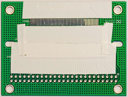
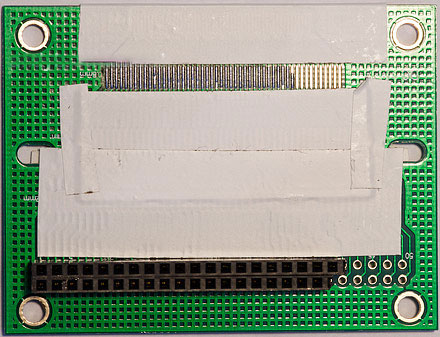
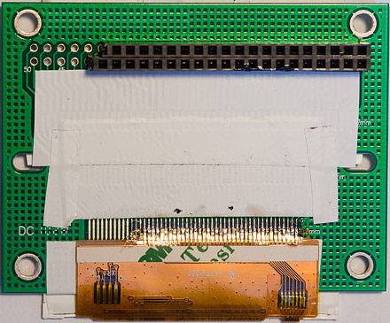
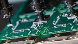
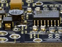
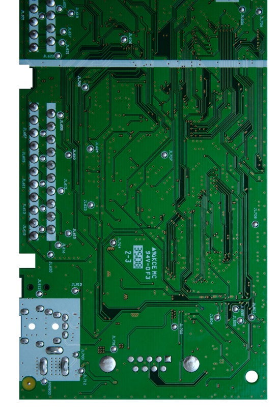
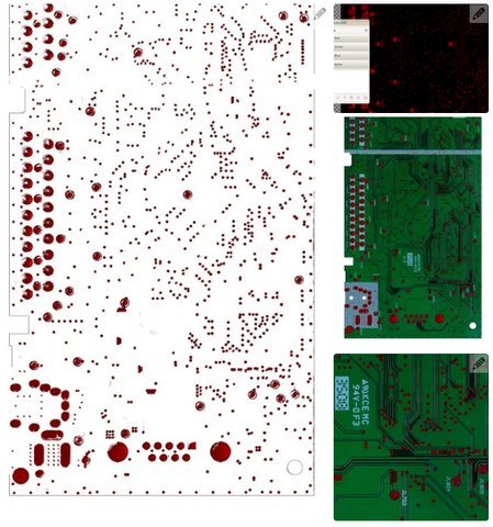
TV PCB
Having knowledge of their names and classification can assist you to quicken the time required to identify them.
In Modern PCB, there is more use of IC chips than passive components, and all the IC chips appear similar (black encapsulation with different shape and size).
For this matter, it is crucial to scrutinize the number printed on the IC chip. Because, without the number, you will require more experience and brain power to decode the PCB.
Some manufacturers will develop mechanisms to delete the number on the chips as a way of hindering reverse engineering of their PCB.
Erasing the lettering reduces the chances of copying their circuit design.
The number is essential since it helps you search for the components’ datasheet from the internet.
The design of most current PCB uses surface mount components, which can be small making it difficult to apply the traditional color band scheme regarding a component such as a resistor.
Number coding similar to the color band scheme is applied for bigger SMD resistor. The first few digits stand for the actual digit as the last digit stands for the number of zeros.
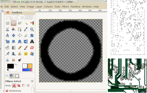
Sample SMD Resistor
Smaller SMD resistors having smaller printed area apply a standard coded system to print their value.
The standard coding system is referred to as EIA marking code. The coding system makes it very difficult to establish the resistor value.
Fortunately, the internet has simplified the task since you only need to search and find the value base on the code.
There also exist apps which enable you to enter the EIA code, and in return gives you the resistance value.
The applications also have extra features which can help you in your PCB reverse engineering process.
Data acquisition is the next stage in reverse engineering PCB and to carry out a successful PCB reverse engineering, get at least two samples of the PCB.
Obtain a detailed scanned image of the populated PCB since this will help you establish the polarities and locations of the components.
Collect the technical manuals and information concerning the PCB assembly. Additionally, obtain usage and maintenance data and performance specifications.
Visually inspect the printed circuit board unit and take note of inconsistency between the available data and the real PCB.
After completing the process of data collection, remove the components from the board. Thereafter, using a thinner, clean the board to remove the solders. Finally, blow dry air to remove dirt and dust from the PCB.
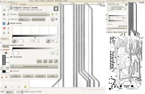
The analysis is the most tedious phase of PCB reverse engineering process.
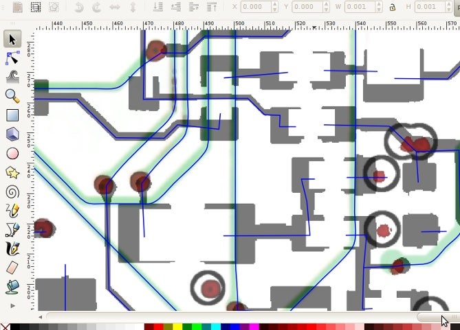
The operation involves the mapping out how the components are interconnected.
You map out the entire connection (referred to as traces) component by component.
However, before commencing the tracing procedure, it is critical to identify the printed circuit board type which is categorized as a single layer, double layer, and multilayer board.
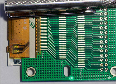
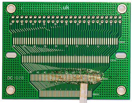
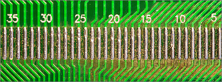
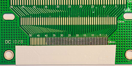
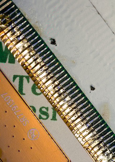
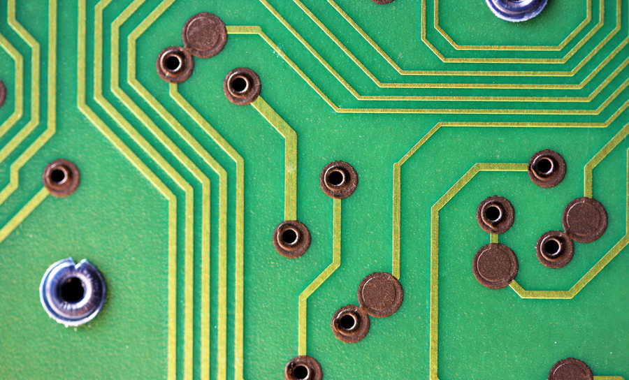
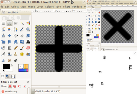
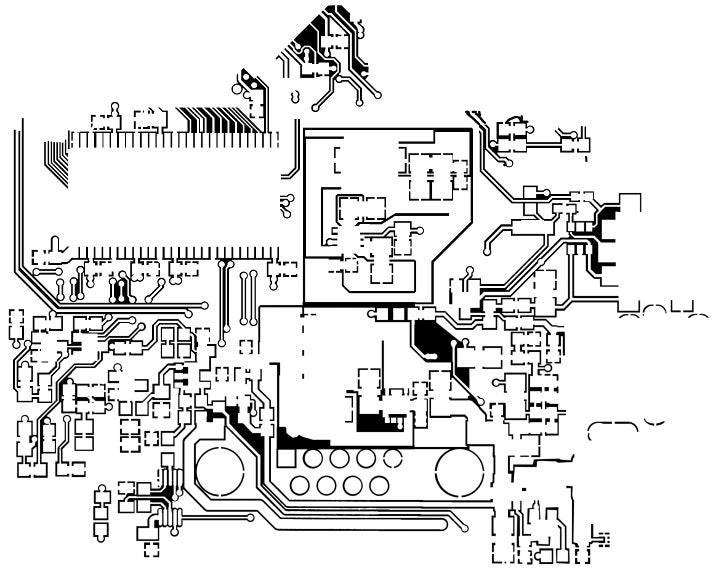
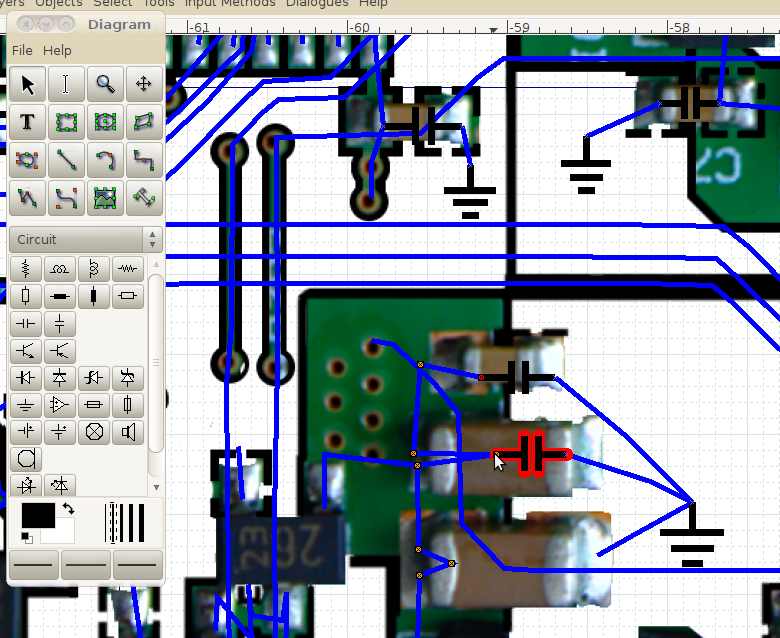
Sample of PCB tracing
Single layer PCB is the simplest circuit board where one face of the board has only the PCB trace routing, while the other face consists of the electronic components.
Single layer board usually contains majorly through-hole components and it is fairly easy to map out the connection.
Double layer PCB is the second type of circuit board where the trace routing can be found on both faces of the board.
In most cases, you will find surface mount components on one face of the board while the through-hole components are placed on the other side.
Usually, traces routing is done beneath the through-hole components and the IC chips.
This type of traces routing makes it impractical to trace out the connection with the naked eye.
You will require a multimeter function continuity (also referred to as continuity tester) to identify a connection.
Typically, it will buzz the moment the probes get in contact with two points connected by a trace.
However, you can as well utilize an Ohm meter function which registers a zero ohm when you probe a connection.
I recommend the buzz since while you concentrate on tracing the circuit, you do not need to check the continuity tester display to confirm a connection.
The buzz sound signal is more convenient.
Even though continuity tester is a convenient device for tracing the connection, it is of essence understanding how it functions.
The buzz is made to sound at a specific ohm threshold.
This implies that a 10 Ohm resistor between two points may result in a buzz, which can mislead you into believing that there is a connection between the two points.
It is therefore important to be aware of this during the probing operation.
Combining the help of your vision and continuity tester should help reduce mistakes.
You should take note of components such as inductors, transformer, a sense resistor (normally bigger than the other types of resistor), coil, and any external wiring or connection to the PCB.
Another popular mistake is probing the trace without unplugging the power supply.
It is important to make sure that you switch off all connections to the printed circuit board before mapping out the connection.
Multilayer PCB is the most complex board to trace.
Commonly for a 4 layer circuit board, most developers prefer to use the middle layer for power traces such as GND and VCC.
Nonetheless, it is not always definite, but there are higher chances based on experience working with different printed circuit boards and common circuit theory.
PCB reverse engineering needs you to reason more like the designer of the circuit board you want to hack.
For a multilayer board, it is almost near impossible to trace the printed circuit board using your normal vision.
In some cases, knowledge of the components coupled with your experience as a designer might help you shorten the procedure.
There will be areas that you will instinctively know that it is not a must you try.
Draw out the position and the connection of the components, mark all the components, and designate the trace the moment you are in a position to establish its function.
Power supply traces are the easiest, to begin with.
This is so since we always know where the power supply is attached to the circuit board.
From there you can trace out where the power connection heads to next.
You will be capable of mapping out the next stage which is commonly the voltage regulator.
However, in the case of an AC power line, you will commonly locate a rectifier before it connects with the voltage regulator.
But this proposal presumes standard design thus it will be upon you to recognize it since there exist many varieties of PCB design.
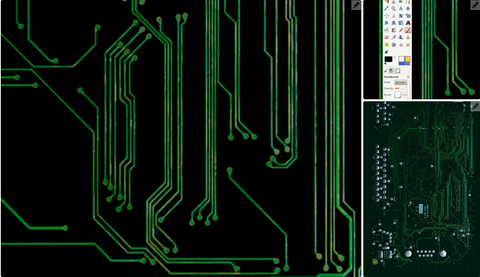
PCB Reverse engineering design
Analysis of the datasheet of the IC chip can also assist you to establish the connection.
Order the component sign into the standard stamp circuit layout that you can identify.
With the configuration, you can easily recognize common standard circuit such as relay circuits, pull up, input circuit, voltage regulator, driver circuit using transistor, among others.
Draw them out in a layout that aids you to identify the circuit module functionality.
The process is complicated, and it is a never an ending conversation on PCB reverse engineering.
]]>1) Draw, scan or photograph the PCB for image preparation
2) Upload pictures
3) Build the layout
4) Create the schematic
After completing these main steps, you should have a full understanding of how the PCB works, which can help you achieve any goal.
1) Record the models, parameters, and locations of all components on the circuit board on paper.
2) Remove components and remove the tin inside the PAD hole. Adjust the contrast and brightness of the canvas until there is a strong contrast between the parts with and without the copper film.Convert two BMP format files into PROTEL format files, and transmit two layers in PROTEL.
3)Convert the BMP of the TOP layer to TOP.PCB. It is to import TOP.PCB and BOT.PCB in PROTEL. They will combine into one picture.
4) Using the laser printer to print the TOP LAYER and BOT LAYER on the transparent film, then put the film on PCBs, comparing whether there is any wrong.
]]>A metal core printed circuit board (MCPCB) also known as thermal PCB, incorporates a metal material as its base as opposed to the traditional FR4, for the heat spreader fragment of the board. Heat builds up due to some electronic components during the operation of the board. The purpose of the metal is to divert this heat away from critical board components and towards less crucial areas such as the metal heatsink backing or metallic core. Hence, these PCBs are apt for thermal management.
In a multilayer MCPCB, the layers will be evenly distributed on each side of the metal core. For instance, in a 12-layer board, the metal core will be at the center with 6 layers on the top and 6 layers at the bottom.
MCPCBs are also referred to as insulated metallic substrate (IMS), insulated metal PCBs (IMPCB), thermal clad PCBs, and metal-clad PCBs. In this article, we will be using the abbreviation MCPCB to avoid ambiguity.
The MCPCBs are made up of thermal insulating layers,metal plates, and metal copper foil.
Accumulation of too much heat in printed circuit boards lead to malfunctions in the devices.
Electronic devices that generate a considerable amount of heat cannot always be cooled using conventional fans. Conductive cooling through metal core boards is an ideal option. In conductive cooling, the heat is transferred from one hot part to a cooler part by direct contact.
This works well since heat constantly seeks to move to any object or medium that is cooler.
100 ohm differential impedance recommended design
90 ohm differential impedance recommended design
Note: Prioritize the use of package ground design. However, if the line is short and there is a complete ground plane, it can be designed without package ground.
Calculation parameters:
FR-4, thickness 1.6mm+/-10%, dielectric constant 4.4+/-0.2, copper thickness 1.0 oz (1.4mil), solder mask thickness 0.6±0.2mil, dielectric constant 3.5+/-0.3.
Fig.1 Design of ground package Fig.2 Design without ground package
100 ohm differential impedance recommended design
line width, spacing 5/7/5mil differential pair and the distance between the pair ≥ 14mil (3W criterion);
Note: It is recommended that the entire group of differential signal lines is shielded with ground, and the distance between the differential signal and the shielded ground line is ≥35mil (in special cases, it cannot be less than 20mil).
90 ohm differential impedance recommended design
line width, spacing 6/6/6mil differential pair, and the distance between the pair ≥12mil (3W criterion).
Note: In the case of a long differential pair trace, it is recommended that the USB differential line wrap the ground at a distance of 6 mils on both sides to reduce the risk of EMI (with and without ground, the line width and line spacing standards are consistent).
Calculation parameters:
FR-4, thickness 1.6mm+/-10%, dielectric constant 4.4+/-0.2, copper thickness 1.0 oz (1.4mil), copper clad substrate(PP) 2116 (4.0-5.0mil), dielectric constant 4.3+/-0.2, solder mask thickness 0.6±0.2mil, dielectric constant 3.5+/-0.3.
Stack-up:
Silkscreen |
Solder mask |
Copper |
Prepreg |
Base material |
Prepreg |
Copper |
Solder mask |
Silkscreen |
The impedance design of the outer trace is the same as that of the four layer board.
The inner trace is generally more plane layer than the surface trace, and the electromagnetic environment is different from the surface.
The following is the third layer trace impedance control recommendation.
100 ohm differential impedance recommended design
line width, spacing 6/10/6mil.
The distance between the differential pair is ≥20mil (3W criterion).
90 ohm differential impedance recommended design
line width,line spacing 8/10/8mil.
The distance between the differential pair is ≥20mil (3W criterion).
Calculation parameters:
FR-4, thickness 1.6mm+/-10%, dielectric constant 4.4+/-0.2, copper thickness 1.0 oz (1.4mil), copper clad substrate(PP) 2116 (4.0-5.0mil), dielectric constant 4.3+/-0.2, solder mask thickness 0.6±0.2mil, dielectric constant 3.5+/-0.3.
Stack-up:
Silkscreen |
Solder mask |
Copper |
Prepreg |
Base material |
Prepreg |
Base material |
Prepreg |
Copper |
Solder mask |
Silkscreen |
Note:
PP types
Type | Dielectric thickness | Adjustable range | Dielectric constant |
1080 | 2.8mil | 2.0-3.0mil | 4.3 |
2116 | 4.2mil | 4.0-5.0mil | 4.3 |
1506 | 6.0mil | 5.5-6.5mil | 4.3 |
7628 | 7.2mil | 7-8.5mil | 4.3 |
Solder mask thickness: 0.6±0.2mil
Cer=3.5+/-0.3
There are three different methods to make the blind hole PCB:
In the traditional multilayer board manufacturing process, the drilling machine is used to set the Z-axis depth for drilling, but there are some concerns:
a.Only one piece can be drilled at a time, and the output is very low.
b.The drilling machine table must be level, and the drilling depth of each spindle must be the same. Otherwise, it is difficult to control the depth of each hole.
c.Electroplating in the hole is difficult, especially if the depth is greater than the hole diameter, it is almost impossible to electroplate in the hole.
Due to the limitations of the processes mentioned above, this method is becoming less popular.
Take an 8-layer PCB board as an example (see Figure )
The Sequential lamination can make blind and buried holes at the same time. First, make the circuit and PTH of the four inner layers (six layers + double layer, top and double bottom layer, and inner four layers). Then laminate the four pieces together into a four-layer board, then make a through-hole. This method has a long process and a higher cost, so it is not universal.
This method is the most popular in the industry, and many domestic manufacturers have similar manufacturing experience.
This method extends the above-mentioned sequential lamination concept, adding layer by layer to the outside of the board and using non-machine-drilled blind holes as the interconnection between the layers. Here are the three main methods:
Gerber files are the output of circuit board design process. These files are utilized for the PCB manufacturing and assembly process. Gerbers provide information about each and every layer in the board stack-up.
Incorrect drill file format: Without the right format of the drill files, it is difficult for circuit board fabricators to import the Gerber file. These files are used to identify the size and location of the hole that has to be drilled. Drill files contain information that can be translated directly to the CNC machine. Many CAD software packages have the option of generating drill files. The header of these files should indicate the format. Such a format is known as a numerically controlled (NC) drill file. They usually have ‘.xln’ or ‘.drl’ or ‘.ile’ extension.
Missing board outline:Gerber files should have a clearly defined board outline. A board outline defines the dimensions of the PCB based on the customer requirement. It gives information about the exact bounds of the board edge which is required by the fabrication machine to route the individual boards from the panel. If the board outline has not been provided, there are high chances that the manufacturing is put on hold by manufacturers.Some CAD software packages don’t produce outlines by default and need to be instructed to produce one. It can be a part of the Gerber file or a general drill file.
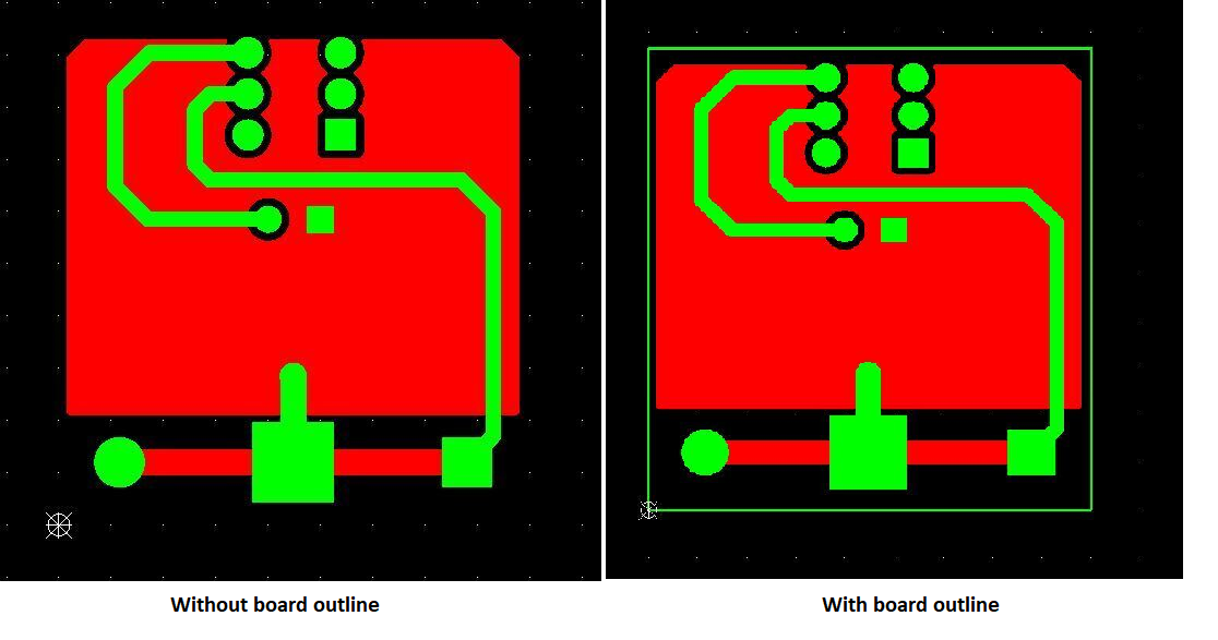
Board outline defined in the Gerber file
Of all the potential problems you may have with your printed circuit boards, Gerber file mistakes are the most inexcusable. While most PCB design errors can be avoided with more careful and focused work, Gerber file errors are the easiest to avoid. Given that the consequences of Gerber file issues can be so expensive and so time-consuming, you simply cannot allow them to happen. A few ways to help you avoid Gerber files problems include:
Staggered vias connect different layers of the board but do not come in direct contact with each other (separate drill axis). Their position is offset on the adjacent layers. Staggered microvias involve fewer design steps. As the second drilled hole is not adjoined with the first one, the laser-drilled vias do not need copper filling. Hence, the design comprises less complicated but time-consuming processes.
The spacing between the laser-drilled holes is the most primitive concern while designing a staggered via. The vertical distance between the centers of two microvias decides whether the staggered via design is possible or not. The vertical separation should be greater than the microvia diameter to arrive at a perfect staggered design.
Manufacturing a board using stacked vias involves more steps than staggered vias. Therefore, it is more complex. Here several vias stacked on top of each other. They connect different layers and occupy less space. Every via is drilled and plated before stacking on top of another. There are two narrow annular rings on the top and the bottom. The upper one signifies the precise registration and the bottom one is used for electrical connection. The design consists of three different actions:
The stacked vias are filled with electroplated copper. It ensures a solid electrical connection and provides structural support. There are occasions when defects can be seen in the deposited copper. Some obstacles are explained below:
It represents a robust PCB testing approach. In-circuit testing often proves costly, though this also depends on the fixture and board size, among other aspects. The ICT test, alternatively inferred as a bed-of-nails test, actuates and powers the specific circuitry on the circuit board. It often entails 100% coverage by design, though it covers about 85-90% coverage in most instances. However, the coverage, albeit not 100%, often comes devoid of any human error.
In-circuit testing deploys fixed probes that get laid out a particular way and which matches the PCB design. It is the probes that check for the solder connection integrity. The ICT tester pushes the circuit board to the bed containing the probes to initiate the test. Predesigned access points exist on the board, allowing the testing probes to connect with the circuit. Consequently, the pressure applied to the connection ensures it all stays intact.
In-circuit testing often gets performed on BGAs (ball grid arrays) or bigger connections. It applies to “mature” products with very little revisions anticipated. However, a lack of DFM (design-for-manufacturing as an objective in your PCB production may make in-circuit testing impossible to carry out. Unfortunately, it is impossible to switch mid-way into an in-circuit approach.
Benefits
The PCB flying probe test is a valuable and less expensive testing option compared to in-circuit testing. It is not powered responsible for checking for shorts, opens, capacitance, diode issues, and resistance. It uses needles attached to the PCB probe on the x-y grid from the basic CAD. However, the ECM program must coordinate and matches the circuit board before running the program.
The flying probe test PCB process is essential in printed circuit board assembly for production and prototype volume testing. It arises from the increasing need for innovative PCB features such as increased board access, test speeds, repeatability, and reliability.
Since it uses PCB test probes that fly, it requires no custom fixtures. However, it is important to note that originally, the design permitted the testing of bare boards. It has since evolved into a go-to, all-encompassing test, ideal for PCB assembly.
Benefits
It is a unique testing approach that uses a 2D or 3D camera in taking pictures of the printed circuit board. The images get relayed into a specific program that compares the board images with a comprehensive schematic. Any board that fails to match the reference schematic at a certain cut-off point gets flagged for inspection.
Automated optical inspection becomes useful in detecting issues promptly and preventing any immediate shut down of the production process. However, the testing approach cannot power up the board and may fail to cover 100% of every part type. Additionally, it is advisable to always rely on other testing approaches besides the AOI. Some of the ideal combinations include the following.
Benefits
It comes with an extra intense testing type for printed circuit boards. By design, it detects any early failures and develops a load capacity. The intensity by which it works can destroy the parts getting tested.
Burn-in testing works by pushing power at its maximum and within the specified capacity through the electronic device. It happens for about 48-168 hours where power gets run through continuous. Whenever a board fails this test, it gets referred to as infant mortality. On this basis, the quota fails to determine the suitability of the PCB’s quality for deployment, especially medical and military applications.
However, burn-in testing is not ideal for every PCB project, as it makes sense for some projects. It can help prevent embarrassing product launches or dangerous products from reaching customers. Burn-in testing has the capability of shortening the lifespan of a product, especially when it subjects your board to undue stress than it can handle. Therefore, you can reduce the test limit to shorter periods to avert overstressing the PCB whenever you cannot identify defects.
Benefits
Popularly inferred to an AXI, the testing approach proves more of an inspection instrument for many electronic contract manufacturers. It entails a testing method where the X-ray technician identifies defects by looking at solder connections, barrels, and internal traces.
X-ray inspection can come either as a 2D or 3D AXI test. The 3D testing provides a quicker testing timeline. The testing process proves capable of checking elements that are not apparent to the naked eye. It can include BGA (ball grid array) packages complete with solder joints and connections. While a useful test, it requires an experienced and trained operator to carry out.
It is also prudent to remember that your electronic contract manufacturer will not necessarily inspect each board layer using the x-ray machine. Yes, you can see through to pinpoint internal defects. However, it is a tedious, expensive, and time-consuming process for ECMs and the client.
Benefits
Most electronic contract manufacturers perform a functional test for verification purposes that the electronic product will power up. It arises since most customers love this old-fashioned testing approach. The test requires external equipment pieces, fixtures, and requirements like MSHA, UL, and other quality standards.
A functional test’s parameters often get specified by the PCB consumer. However, some electronic contract manufacturers can assist with the development and designing of such tests. It also takes time and may not prove ideal if you need to quickly get your PCB product to the market. However, it can come in handy in saving face and money from a longevity and quality standpoint.
Benefits
Other functional test types can apply when checking a printed circuit board project based on the prevailing circumstances. The functional test can vary since a functional test aims to test and verify the PCB’s behavior when deployed. Aspects such as the PCB’s development besides procedures vary from one type to the other.
Other functional tests that apply based on the PCB variations include the following,
Benefits
The birth and development of FPC and PCB gave birth to the new product of flexible and rigid printed circuit board.
Soft and hard bonding plate is the flexible circuit board and hard circuit board through the compaction and other processes, according to the relevant process requirements combined to form a FPC characteristics and PCB characteristics of the circuit board.
Because the soft and hard bonding plate is a combination of flex pcb and PCB, the production of soft and hard bonding plate should have both FPC production equipment and PCB production equipment.
1. Electronic engineers draw the trace and layout of the soft bonding plate according to requirements.
2. Issued to the production of Flex-rigid PCB board factory, after the CAM engineer dealing and planning with the relevant documents, then arrange the FPC production line to produce the required FPC, PCB production line to produce PCB, these two soft board and hard plate out after that,in accordance with the planning requirements of electronic engineers, the FPC and PCB through the compressor seamless compaction.
3. After a series of detailed links, the final process of the soft and hard bonding board.
One of the most important part, is the Test of flex-rigid PCB board , There are many details need to be confirmed before shipping, generally have to carry out a full inspection, so as not to allow both supply and demand to cause the loss of related benefits, so the value is relatively high.
Such as manufacturing progress of 6-layer Flex-rigid PCB:
Advantages: Soft and hard bonding plate at the same time has the characteristics of FPC and PCB characteristics, therefore, it can be used in some products with special requirements, both a certain flexible area, but also a certain number of rigid areas, to save the interior space of products, reduce the volume of finished products, improve product performance has a great help.
Disadvantages: The production process of Flex-rigid PCB boards are numerous, the production is difficult, the yield is low, the pcb materials and manpower wasted more. Therefore, the price is relatively expensive and the production cycle is relatively long.
]]>2. Cutting material — cutting machine, baking oven
3. Laminating – browning production line, laminating machine, grinding machine
4.Drilling – CNC drilling machine
5.Grinding plate—grinding machine
6.Metallized holes (PTH) – chemical copper production line (sink copper line)
7.Graphics transfer – film machine, UV exposure machine or LDI
8.Graphic plating – electroplating production line
9.Faded (wet) film – fade film production line
10.Graphic etching —- etching production line
11.Solder mask production — screen printing machine, UV exposure machine or LDI
12.Baking curing – oven, tunnel furnace
13.Surface treatment—OSP production line or chemical nickel gold wire, chemical nickel-palladium gold wire
14. Forming—punching machine or CNC boring machine, cutting machine
15.Test — electric measuring machine, AOI, 3DAOI.
A good PCB board has a lot to do with PCB production equipment, especially for some difficult boards, and the requirements for equipment are even higher.