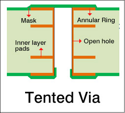
Tenting vias
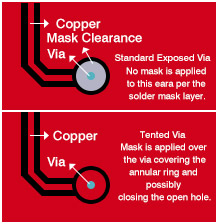
It’s the most popular and mature process in PCB fabrication, and tenting vias mean to cover the annular ring and via hole with solder mask, which is mainly in covering the annular ring to prevent exposure to the elements and reduce accidental shorting or contact with the the circuit. No special steps are taken to ensure the hole opening remains closed. Sometimes tenting vias will lead to the hole remaining covered but there is no guarantee, and smaller diameter vias (12mil diameter or less) have the best chance of remaining closed. However it will make an effect on the PCB fabrication process if there is not solder mask ink in the vias.
Plugged vias
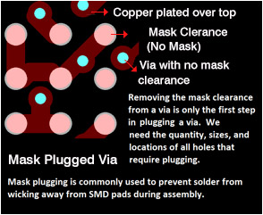
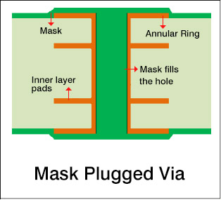
Plugged hole is a process in PCB fabrication, which filled with ink in the vias, not solder ball and white light, as a matter of principle the diameter vias( 0.5mm or less) have the demands of the plugged vias. Plugged vias, taking specific measures to ensure the via is plugged and sealed with mask and the annular ring is covered, and it can solve the problem of being yellowing of the aperture but the tenting vias can’t do, however the cost is excessively high. Plugged hole is mainly in a BGA design where vias are usually found in very close proximity to the BGA’s SMD pads. What should it concern is that solder will far away from the intended pad and flow down the via creating poor or non-existent solder joints during assembly.
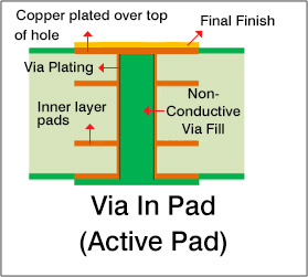
Via In Pad (Active Pad)
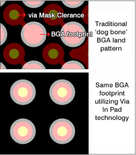
Via in pad, the annular ring of via is exposing with HAL( such as the components pad exposes), it is without any treatment in PCB fabrication. However now via in pad is more and more normal with BGA packages are becoming tighter. And not using the standard “dog bone” land pattern to transfer signal from the BGA footprint to a via that passes signal to other layers, vias can be drilled directly into the BGA footprint pads. This allows much simpler routing by soldering directly over the via. Make sure this process is called out in your fab notes. Via in pad is usually used for testing the signal, but it’s easy to result in the short.
