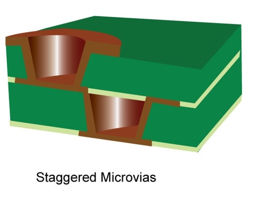
What are staggered vias?
Staggered vias connect different layers of the board but do not come in direct contact with each other (separate drill axis). Their position is offset on the adjacent layers. Staggered microvias involve fewer design steps. As the second drilled hole is not adjoined with the first one, the laser-drilled vias do not need copper filling. Hence, the design comprises less complicated but time-consuming processes.
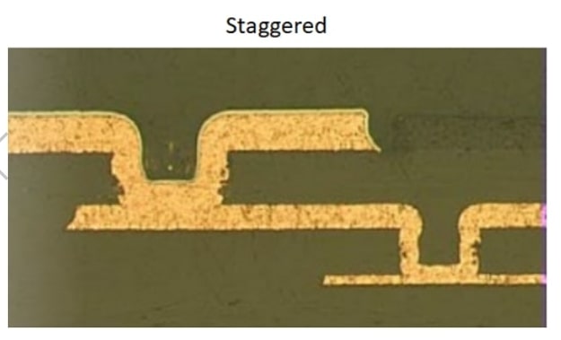
The spacing between the laser-drilled holes is the most primitive concern while designing a staggered via. The vertical distance between the centers of two microvias decides whether the staggered via design is possible or not. The vertical separation should be greater than the microvia diameter to arrive at a perfect staggered design.
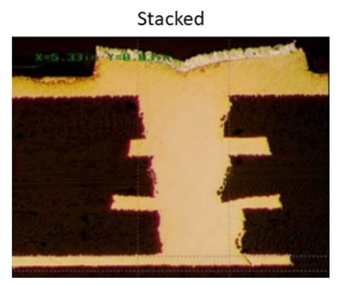
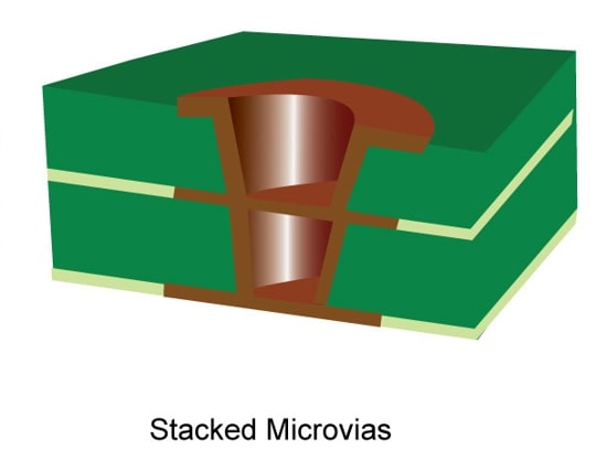
What are stacked vias?
Manufacturing a board using stacked vias involves more steps than staggered vias. Therefore, it is more complex. Here several vias stacked on top of each other. They connect different layers and occupy less space. Every via is drilled and plated before stacking on top of another. There are two narrow annular rings on the top and the bottom. The upper one signifies the precise registration and the bottom one is used for electrical connection. The design consists of three different actions:
- Hole filling with copper
- Planarization
- Extra imaging
Copper filling of stacked vias
The stacked vias are filled with electroplated copper. It ensures a solid electrical connection and provides structural support. There are occasions when defects can be seen in the deposited copper. Some obstacles are explained below:
- The improper deposition of copper can create voids in the vias. These voids generate localized stress within the structure. This can hamper the reliability of the stacked microvias.
- Low-grade electroless copper results in inferior bonding between the base of the microvia and the target pad under it.