
Several tests are available that fulfill the quality standards such as visual, manual, and X-ray inspection. Each test has its specification levels that range from measuring different parameters to finding missing parameters.
Manual inspection
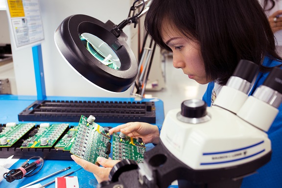
Manual inspection or visual inspection is the simplest method of inspecting a circuit board. To conduct this test, one can examine the board either with the naked eye or through a magnifying glass. It includes the comparison of the board with the design documents to ensure that the specifications are met. Types of defects vary according to the kind of board and the components mounted on it.
The checklist for manual inspection includes the following elements:
- Verifying the board’s warpage.
- Measuring the dimensions of an assembly according to the customer’s specifications.
- Confirming component solder joints are free of solder bridges, open solder, cold solder, etc. as per IPC or customer-defined workmanship.
- Inspecting PCB surface for pits, scratches, dents, pinholes, and other defects.
- Ensuring there is no component damage and no incorrect component mounting orientation.
- Other requirements as specified.
However, the scope of this method is limited. There are certain drawbacks.
- Manual inspection is time-consuming and expensive. It does not assure high quality.
- With miniaturization and technological advancements, the board requires high-level techniques for inspection.
AOI inspection
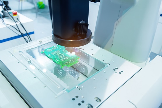
Automated optical inspection is a widely used method for inspecting devices under test (DUT) to examine various surface feature defects such as open circuits, short circuits, etc. This technique is used in circuit board manufacturing as well as assembly. This system comprises illumination, a machine vision camera, and processing software.
A machine vision camera scans the circuit board and looks for defects. Since the process requires proper illumination, the AOI machine uses LED lighting that provides optimum lighting for accurate verification of different parts. The processing software employs two methods: the golden board standard and algorithm-based programming.
AOI inspection detects errors such as:
- Solder shorts, and open circuits
- Components with incorrect marking, missing, or skewed
- Misplaced chips, or chip-orientation defects
- Violations of component spacing.
- Offsets and polarity of components
- Excessive and insufficient solder joints
- Flipped parts
- Defects in specific areas
AOI inspection differs based upon the 2-D and 3-D evaluating machines.
Board manufacturers can detect coplanarity with 3D inspection on height-sensitive devices without a problem, although shadows may cause issues in some board layouts.
X-ray inspection
X-ray inspection or automated X-ray inspection is the most reliable tool for finding invisible errors in circuit boards with ICs (CSP: chip-scale package) and BGAs. It can scan and detect large voids and cracks. This method can access internal geometries and structural compositions without causing any damage. The test is performed in the same way as AOI by capturing images.
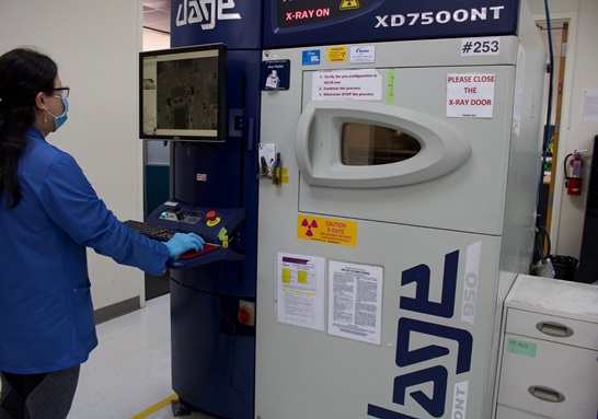
X-ray inspection system identifies voids within solder joints that are not visible to AOI.
This system can determine faults like:
- Soldering defects: Solder bridges, open solder, insufficient solder, excess solder, and poor solder quality
- Component defects: Lifted lead, missing components, and misplaced components
The X-ray inspection method is beneficial when BGA, CSP, and similar packages are used, as the error detection in such cases exceeds the capabilities of AOI.
In-circuit test
In-circuit test (ICT) involves testing populated PCBs to examine their resistance, capacitance, shorts, opens, and other electrical quantities to ensure a sound fabrication. It is possible to conduct this test with either a bed of nails fixture or a flying probe tester.

ICT tests the following:
- Dimensions of components, leads, and lands
- Markings on components
- Problems with soldering
- Shorts between traces and component leads
- Circuits with open connections (opens)
- Values of the resistors
- Passive components check
- Active components check
- Misoriented analog and digital components
- Values of capacitance and inductance
- Incorrect or missing components
Despite this, ICT cannot check multiple power connections, decoupling capacitors, mechanical fixings, and redundant power connections. Even though the testing method has its flaws, it remains one of the most effective ways to test a circuit board assembly.
Functional test
Performing functional testing on finished PCBs is the last step before approving the product. Functional testing is the most comprehensive way to determine if a manufactured board is ready for dispatch.
This test can identify the following signal problems:
- Power integrity issues – excessive ripple of power distribution network (PDN), low-frequency noise, and excessive jitter
- Various signal distortion issues, such as signal skew in buses and excessive distortion on several nets
- Due to incorrect component placement, a missing component, or excessive IR drop, the board might display incorrect voltage or current
Functional testing is not always accurate. There are many variabilities, including inputs, testing procedures, test plans, an outline of the desired results, and testing parameters. These variabilities make this testing method very complex.