
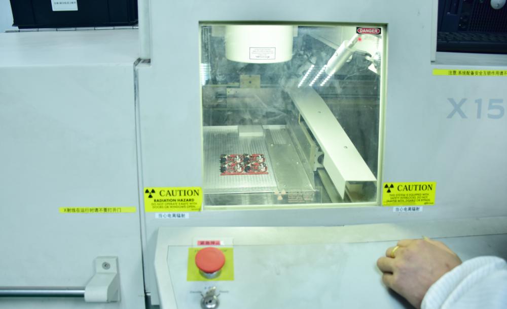
X-Ray inspection: X-ray inspection uses high power that generates from cathode rays to strike metal. X-ray appeared to lose kinetic energy from electronic slow down suddenly. The position that can’t be inspected will use an x-ray to inspect the change of light intensity. The image will show the inner structure to find out which area or position has the problem.
With the rapid development of electronic technology, SMT technology is already universal. The chips’ footprint is smaller with more pins, especially when BGA came out in recent years. The BGA design is not like the conventional design with pins distributed all around, but distributed at the bottom of the chips. There is no doubt that it is difficult to determine whether the soldering work is good or not by traditional artificial visual examination.
That is why we must conduct ICT and functional tests. It is hard to fix if bad solder work is found at mass production. Artificial vision is a technology which the lowest precision and repeatable results. The X-ray test is widely used in SMT reflow soldering work inspection and can analyze qualitative and quantitative solder joints, and determine the fault and repair it in time.
X-ray inspection application :IC, BGA, PCB/PCBA, SMT inspect, etc.
Test steps: Confirm the type of material of sample → sample put on PCB x-ray machine → analyze the image → marked the fault position and type.
Reference standard:《IPC-A-610E acceptability of electronic assemblies》,《GB/T 17359-1998General specification of X-ray EDS quantitative analysis for EPMA and SEM》
BGA X-ray Inspect list :
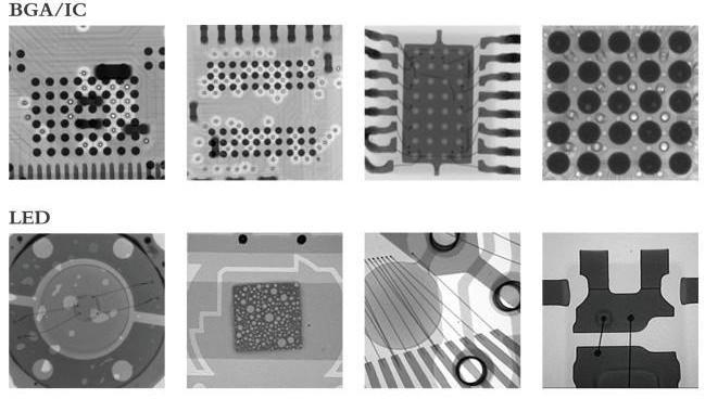
1、IC’s footprint inspection: Peel, cracking, empty, wire bonding.
2、Print circuit boards fabrication inspection: Welding line offset bridging, open circuit.
3、SMT weldability inspection: Solder joints empty inspection and measurement.
4、Circuit line inspection: Open circuit, short circuit, defective or fault connection.
5、 Integrity inspection of solder ball in array package and chip covering packaging.
X-ray inspection devices have seen fast development in recent years; it now has 3D inspection from the previous 2D generation. 2D is transmission x-ray inspection, and it can clear an image of the solder joints and on which single layer PCB. However, it is inadequate for 2 layer reflow soldering PCB because two side solder joints image is overlapped, and difficult to find faults. However, 3D inspection is lamination technology that focused on all layers, and the corresponding image is projected onto a high-speed rotating receiving surface
Since the high-speed rotation of the receiving surface makes the image focal point very clear and the image on the other layers is eliminated. The 3D inspection method can image the solder joints independently on both sides of the plate.
In addition to examining double-sided soldered plates, 3D X-ray can also perform multi-layer image “slicing” inspection of invisible solder joints such as BGA, which is a thorough inspection of the top, middle, and bottom of the BGA solder ball joints.
Simultaneously, this method can also be used to measure through hole (PTH) solder joint, check whether the solder material in the through hole is full, to improve the joint quality of the solder joint significantly. The SPC statistical control function can be connected with the assembly equipment to achieve real-time monitoring of assembly quality
All X-ray inspect machines have the below characteristics no matter if it’s 2D or 3D:
(1) The machine has an X-ray tube that creates X-ray.
(2) The sample is moving on the X-ray machine to inspect each sample position and adjust magnification and inspect the inclination angle.
(3) A device can receive an image that is captured through x-ray.
The advantages of using X-Ray inspection equipment as below :
(1) The inspection effectiveness rate is about 97%, and such defects can be inspected: Cool solder, tin connect, not enough solder, components missing, etc. In particular, an X-Ray can also check BGA, CSP, and other hidden solder joint devices
(2) High test range, X-ray can test inside of the sample.
(3) Short inspection time.
(4) Find defects that cannot be reliably detected by other testing methods, such as cool solder, air holes, and poor forming.
(5) Only need to inspect 2-layer or multi-layer once.
(6) Provide measurement information to evaluate the production process, such as solder paste thickness, solder amount under the solder joint, etc.
