
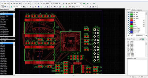
Process 1# : PCB Design and Gerber file
The circuit designer draws schematics in CAD software that will be used to layout the PCB design. The designer must coordinate with the PCB manufacturer about the software used to layout the PCB design so that there will be no compatibility issues. The most popular CAD PCB design software is Altium Designer, Eagle, ORCAD and Mentor PADS.
After the PCB design has been accepted for fabrication, the designer will generate a file from the design that is accepted by the PCB manufacturers. This file is called “GERBER file”. The Gerber file is the standard file used by majority PCB fabricators to show the components of PCB layout like copper tracking layers, and solder mask etc. The Gerber file is the 2D vector image file. The extended Gerber delivers perfect output.
The software has the user/designer defined algorithm that has key elements like track width, board edge spacing , trace and hole spacing and hole size. This algorithm is run by the designer to check for any errors in the design. After the design is verified, it is sent to PCB fabrication house where a DFM check is performed. The DFM (Design for Manufacturing) check is used to assure the minimum tolerance in PCB design.
Process 2 # : GERBER to Photo Film
The special printers used to print the PCB photo film is called “plotter”. These plotters will print circuit boards the films. These films are used to image the PCB. Plotters are very accurate in printing technology to give a highly detailed film of PCB design.
The plastic sheet come out from the plotter is the PCB printed with black ink. In case inner layer, the black ink represents the conductive copper track while the blank portion is non-conductive part. On the other hand, for outer layer, the black ink will be etched away and blank area is for copper. These films should be stored properly to avoid unnecessary contacts or fingerprints.
Each layer has its own film sheet. Solder mask has a separate film. All these films must be aligned together to draw a PCB alignment. This PCB alignment is achieved by adjusting the table on which the film sheets are fit, and after a small calibration of table the optimum alignment is attained. The films must have registration holes to sit accurately upon each other. The registration pins will fit in the registration holes.
Process 3 # : Inner layer printing: Photo resists and Copper
Now these photo films are printed on copper foil. The basic structure of PCB is made of a laminate board. The core material is epoxy resin and glass fiber known as substrate material. Laminate receives the copper that construct the PCB.pcb Substrate gives a strong platform for the PCB. Copper is covered on both sides. The process involves removing away the copper to show up the design from the films.
The decontaminated environment is very important to clean the PCB from copper laminate. It must be ensured that no dust particle lie on the PCB otherwise it will cause circuit to short or open
Now the photo resist film is applied. The photo resist is made of photo sensitive chemical which will harden when Ultra Violet radiation is applied. It must be ensured that the photo films and photo resist films must match exactly upon each other.
These photo film and photo resist film are settled on the laminate board by holding pins. Now UV radiation is applied. The black ink on the photo film will block the UV light thus preventing the copper underneath it and not hardening the photo resist under the black ink traces. The clear area will pass the UV light thus hardening the excess photo resist which will be removed.
The board is then washed with alkaline solution to remove excess photo resist. The board will now dry.
The PCB now is available with resist covering the copper used to make tracks of circuit. If the board is two layers pcb then it will go for drilling otherwise for multilayer the more steps to come.
Process 4 # : Removing the Unwanted Copper
A powerful copper solvent solution is used to remove the excess copper just as alkaline solution removed the excess photo resist. The copper that is under the hardened photo resist will not be removed.
Now the hardened photo resist will be removed that protected the desired copper. This is achieved by washing off the PCB with another solvent.
Process 5 #: Layer Alignment and Optical Inspection
After all the layers are ready from above mentioned steps, they are then aligned upon each other. This can be done by punching registration holes as mentioned in previous step. The technician will place all layers in the machine known as “optical punch”. This machine will punch the holes accurately.
Layers ones placed and error occurred cannot be reversed.
The automatic optical inspection machine will detect any defects using laser and compare the digital image with Gerber file.
Process 6: Layer-up and Bonding
At this stage all of the layers including the outer layer will be bonded together one upon each other. All the layers will be stacked upon substrate.
The outer layer is made of fiber glass “pre-impregnated” with epoxy resin called prepreg. Top and bottom of the substrate will be covered with thin copper layer having the copper trace etching.
A heavy steel table with metallic clamps is used for bonding/pressing layers. The layers are tightly secured with the table to avoid movement during alignment.
A prepreg layer is fit over alignment table, then the substrate layer fits upon it, then copper sheet is placed. More prepreg sheets are placed similarly and finally aluminum foil complete the stack.
A computer will automate the process of bond press, heating the stack and cooling at controlled rate.
Now the technician will remove the packing pins and pressure plates to unpack the stack.
Process 7: Drilling
Now it is time to bore the holes in stack PCB. The precision drill achieves 100 microns diameter holes, with great accuracy. This drill is air driven drill has a spindle speed around 300K RPM. But even with this speed the drilling process takes time because each hole takes its time to be bored perfectly. The x-ray based identifier spots the drill locations accurately.
The drill files are also generated by PCB designer that is given to PCB fabrication house at earlier stage. This drill file determines the micro movement of drill and spots where to bore holes. These holes will now become vias and holes after plating.
After carefully cleaning, the PCB panel is now treated with chemical deposition. During this a thin layer (1 micron thick) of copper is deposited over the surface of the panel. The copper flows into the drilled holes. The walls of the holes are entirely plated with copper. The whole process of dipping and removal is computer controlled

Process 9 #: Outer Layer Imaging
Same as for the inner layers, the photo resist is applied to the outer layer, the prepreg panel and black ink film joined together is now blasted with UV rays in yellow room. The photo resist hardens. The panel now goes through the machine to wash away hardened resist protected by black ink opacity.
Process 10: Plating of Outer Layer:
Electroplate panel with thin layer of copper. After initial copper plating, the panel gets tin plating, which allows removal of all the copper left on the board. The tin prevents the part of the panel required to remain enclosed with copper during the etching stage. Etching eliminated undesired copper from the panel.
Process 11: Etching
The unwanted copper and copper under the residual resist layer will be removed. Chemical are used to clean the surplus copper. On the other hand tin covers the desired copper. It now finally results in proper connections and tracks
Process 12: Solder Mask Application
The panels are cleaned and epoxy solder mask ink will cover the panel. The UV radiation is imposed on board that goes through the solder mask photo film. Covered sections stay unhardened and will be removed. The board is now put in oven to heal solder mask.
Process 13: Surface Finish
The HASL (Hot Air Solder Leveling) gives extra ability to the PCB for solder. The RayPCB provides immersion gold and immersion silver HASL. The HASL gives uniform pads. This leads to surface finish.
Process 14 # : Silkscreen
The PCB is in its final stage receives ink-jet printing/writing on surface. This is used to indicate important information related to the PCB.

Process 15 #:Electrical Test
Final stage is electrical testing of final PCB. The automatic process validates the functionality of PCB to match the original design. At RayPCB, we offer Flying Probe Testing or Nails Bed testing.