
Impedance Matching in PCB Design
It is fair to consider a PCB itself as a component in which multiple traces are connected. Each trace is different, some are high speed, some are low speed, some are noisy, some are used by the return path of circuit current, etc. Now, as we all know, there are lots of variations in ideal circuits and real circuits. Suppose a high-frequency trace is routed with a 7mm copper trace with a 0.5mm track width, it will add Inductance, Capacitance, and resistance on the track. This makes a difficult situation for high-frequency signal lines as that capacitance and inductance could change the frequency of the signal and the ending point of the trace will produce completely different results than the starting point of the trace. The major degradation of this type of signal is due to the Impedance in PCB trace.
What is Impedance?
You can think of Impedance as resistance in AC. Impedance is also measured in Ohms, just like Resistance, but it is very different from resistance. Resistance Ohms works in DC characteristics, but the impedance is used in AC, specifically, that has a frequency.
To ensure that the signal trace is carefully designed and the quality of the signal does not degrade over the traces, impedance needs to be controlled carefully as the impedance of the traces of a PCB is generally uncontrolled.
Importance of Impedance Matching in PCB Design
Essentially, impedance control in PCB design refers to the matching of substrate material properties with trace dimensions and locations to ensure the impedance of a trace’s signal is within a certain percentage of a specific value. Controlled impedance boards provide repeatable high-frequency performance.
Following are the reasons to control impedance in PCB design.
- At high-frequency, the signal traced on a PCB is not just a connection but acts like a component. Even a single trace has different characteristics at different points.
- Whenever the signal moves further in the traces, different impedance produces signal reflection that is dependent on the difference between two unmatched impedances. The larger impedance mismatch produces larger reflection and affects the signal integrity.
The reflection of the signal superimposes the actual or primary signal that is often misunderstood by the high-frequency ADC, high-speed processing circuits, and fails to decode the actual signal.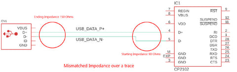
Standard Impedance Values for PCB Design
Different signal traces require different impedance characteristics over the entire signal traces. Depending on the types of signal and the speed of the data transfer or frequency, the list below will give a widely accepted controlled impedance for different PCB signal traces.
It is important to remember that the Impedance needs to be maintained all over the signal path.
| Signal Standard | Targeted Impedance (Ohms) | Accepted Tolerances |
| USB | 90 | +/- 15% |
| HDMI | 95 | +/- 15% |
| IEEE 1394 | 108 | +/- 2% |
| Displayport | 100 | +/- 20% |
| VGA | 75 | +/- 5% |
| DVI | 95 | +/- 15% |
| PCIe | 85 | +/- 15% |
| Ethernet Cat.5 | 100 | +/- 5% |
Thus, when routing signal traces, it is important to maintain the above impedances to maintain signal integrity.
However, other than this, specific impedance requirements are always mentioned in the datasheet of the respective component. It is advisable to go through the datasheet to get information about high-frequency traces and what are the impedance requirements of the particular signal.