This project is a result of needing to service a domestic electronic item without being able to obtain a circuit diagram.
The process proved to be very long and painstaking, but also very rewarding. The steps presented here are not exact, and you will no doubt find your own way of working which is more effective in the case of any particular board. However, I believe the basic procedure is essentially correct for the majority of boards which are too complex to reliably hand trace. Without the need to invent the process, things should progress more quickly.
For simple boards, it is probably better to use pencil and paper to draw the board onto squared paper, replacing components with their symbols, and changing track crossing places to avoid components.
For complex boards, it is too easy to lose your place using this method. The next "level" of complexity from a simple, drawable board, would probably be a good candidate for the tracing methods described in step 16 of this instructable, missing out all the image editing procedures, and modified accordingly.
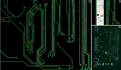
At a higher level of complexity, as on the board shown in this project, I decided there were too many tracks for hand tracing to be reliable, and used the graphical techniques described. These methods arise partly from the photographs I took being too unevenly lit and inadequately sharp. Better photos means less work.
All the editing was done on a laptop running Linux. Windows versions are available of the main tools, Gimp, Inkscape, AutoTrace and Dia, but I don't know if a Windows version is available of the utility pstoedit, needed for an unfortunate extra workaround step. I'm sure another workaround can be found, if it isn't.
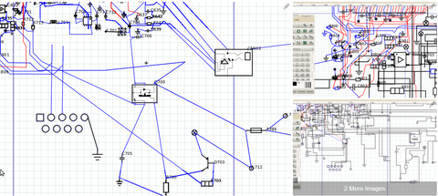
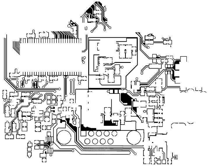
I also discovered as a result of this project that completely hidden traces can exist - in my diagram there is a transistor with it's base apparently unconnected, but I can't find a connection or through hole for it. I assume it's completely hidden in some way.
I'm pleased to say that after creating the diagram, I was able to use it to confirm the suspected faulty part.
Addendum: since writing this instructable I have discovered there are such things as "blind vias" - where the hole only goes part-way through the pcb and is connected to an inner layer only. It would appear that the board I worked on here utilises these, as a number of components appear to be missing connections. I believe, unfortunately, that these are hidden in the SMD pads themselves, so impossible to find without de-soldering. So if you end up with an incomplete looking schematic, that could well be why. Google for "blind pcb vias" to learn more.
STEP 1: TOOLS AND EQUIPMENT

You will be working from photographs, and need some software.
You need:
* A good camera, preferably with a tripod
* Even lighting - a badly lit picture will cause a lot of extra work. A bounced flash is only just good enough. A ring flash may be your best option if you have access to one.
* A computer
* Internet access, to look up components (but see note)
* A multimeter - not essential, but helpful (depending on how precisely you need to know how the circuit works, if you are dealing with SMD's, the ability to measure capacitance could prove useful)
* A strong magnifying glass - you may need to check details which you can't make out from the photos.
* A photo editing program. I use the Gimp, which is free, and these instructions are Gimp-specific. I also used the vector program, Inkscape, to clean up the lines.
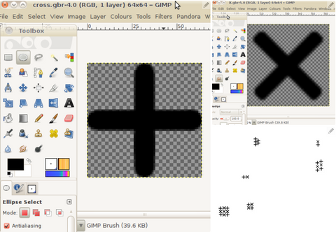
* A program to turn the photo into a vector line-drawing. I use AutoTrace, which is free. I chose AutoTrace specifically because it has a "centre-line" option, originally designed to help pick out text in an image, but ideal for this job. I found AutoTrace picks up too much detail to be useful for general cleaning up though.
* A program to manipulate vectors. I use Inkscape, which is free, and these instructions are Inkscape specific.
* A program to draw manipulate diagrams. I use Dia, which is free, and comes with an excellent set of component symbols (but see caveat, in step 18)
* As the current version of Dia has a problem importing svg files, and an intermediate program, pstoedit, was needed.
* A graphics tablet is a big help, I discovered, especially for hand-tracing some of the tracks.
* Lots and lots of time and patience...
STEP 2: GETTING PHOTOS
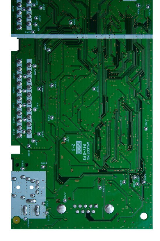
STEP 3: CLEAN UP THE PHOTOS

STEP 4: RESCUE THE HOLES
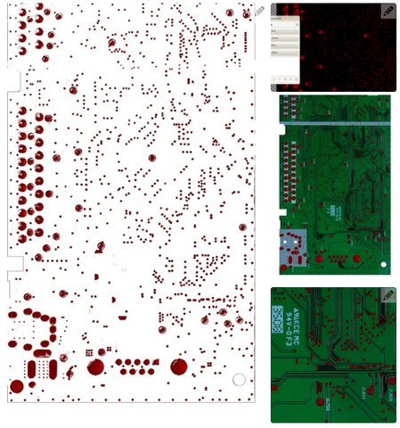
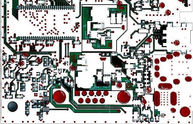
STEP 5: CIRCLE THE GROUND PLANE HOLES
STEP 6: MARK THE FREE HOLES
STEP 7: REMOVE GROUND-PLANES

STEP 8: PAINTED AREAS


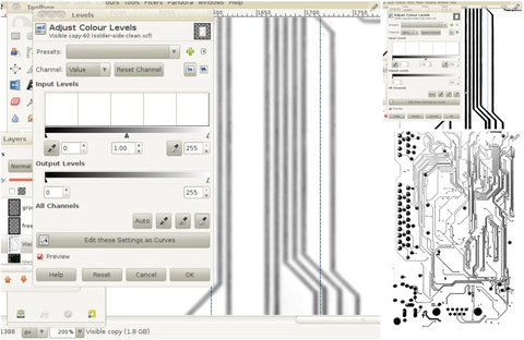
STEP 9: CLEAN THE TRACKS
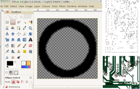
STEP 10: REVERSE AND BURN OUT
STEP 11: SMOOTH THE EDGES

STEP 12: AUTOTRACE

STEP 13: COMPONENT SIDE

STEP 14: FILL IN THE SUBSTRATE
STEP 15: ISOLATE THE COMPONENTS
STEP 16: COMBINE THE SIDES
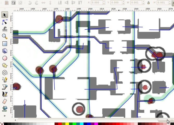
STEP 17: ADD COMPONENT SYMBOLS
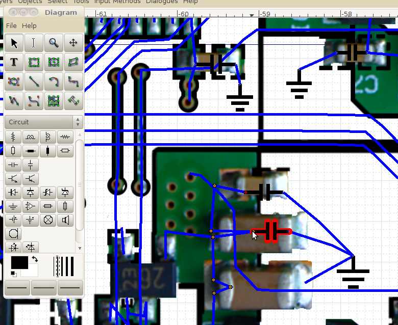
STEP 18: FINALLY, REARRANGE