
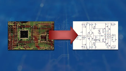
Reverse engineering a print circuit board is a long process, but it’s worth to explore, so reverse engineering a PCB should follow the following main stages:
1) Draw, scan or photograph the PCB for image preparation
2) Upload pictures
3) Build the layout
4) Create the schematic
After completing these main steps, you should have a full understanding of how the PCB works, which can help you achieve any goal.
PCB Reverse Engineering Regular Flow Process
1) Record the models, parameters, and locations of all components on the circuit board on paper.
2) Remove components and remove the tin inside the PAD hole. Adjust the contrast and brightness of the canvas until there is a strong contrast between the parts with and without the copper film.Convert two BMP format files into PROTEL format files, and transmit two layers in PROTEL.
3)Convert the BMP of the TOP layer to TOP.PCB. It is to import TOP.PCB and BOT.PCB in PROTEL. They will combine into one picture.
4) Using the laser printer to print the TOP LAYER and BOT LAYER on the transparent film, then put the film on PCBs, comparing whether there is any wrong.