
What is a controlled impedance?
Controlled impedance is the characteristic impedance of a transmission line formed by PCB traces and its associated reference planes. It is relevant when high-frequency signals are propagating on the PCB transmission lines. Controlled impedance is important for solving signal integrity problems, which is the propagation of signals without distortion.
The impedance of circuits is determined by the physical dimensions and the dielectric materials of the PCB. It is measured in Ohms (Ω). Types of PCB transmission lines that require controlled impedance are single-ended microstrip, single-ended stripline, microstrip differential pair, stripline differential pair, embedded microstrip, and co-planar (single-ended and differential)
Why do you need controlled impedance?
Typically, you will need controlled impedance for PCBs used in high-speed digital applications, such as RF communication, telecommunications, computing using signal frequencies above 100MHz high-speed signal processing, and high-quality analog video such as DDR, HDMI, Gigabit Ethernet, etc.
At high-frequency, the signal traces on a PCB act like transmission lines, which have impedance at each point on the signal trace trajectory. If this impedance varies from one point to the next one, there will be a signal reflection whose magnitude will depend on the difference between the two impedances. The larger the difference is, the greater the reflection will be. This reflection will travel in the opposite direction of the signal, which means that the reflected signal will superimpose on the primary signal.
As a result, the original signal will be distorted: the signal intended to be sent from the transmitter side would have changed once it gets to the receiver side. The distortion may be so much that the signal may not be able to perform the desired function. Therefore, to have undistorted signal travel, the PCB signal traces must have a uniform controlled impedance to minimize signal distortions caused by reflections. This is the first step to improve the integrity of the signals on the PCB traces. For better understanding, read the effects of high-speed signals in a PCB design.
A uniform transmission line on a PCB has a definite trace width and height and is at a uniform distance from the return path conductor, usually a plane at a certain distance from the signal trace.
Factors that affect the controlled impedance
Factors that influence the PCB impedance tolerances include materials’ resin content percentage, Dk values of the resin and the type of the glass cloth used, and other physical PCB tolerances like trace height and width at the top and bottom of the trace. When you give Sierra your PCB design– copper patterns, hole patterns, and final material thicknesses– we laminate the copper layers into a single circuit board. We manufacture your PCB with the right pattern sizes and positions within certain tolerances. You must ensure that your manufacturer provides you the right size, position, and tolerance of your etched features. If not, your boards will vary from each other, making debugging performance-related issues very difficult.
Why is it good to specify the dielectric of the board instead of CI?
The impedance of traces is also defined by the PCB materials used on the board. The dielectric constant of the materials and the expected impedance based on certain parameters is called a controlled dielectric. If you like math, you can take the controlled dielectric approach to control the impedance you need. Once you make your calculations, you can specify the dielectric space required between the copper layers in your fab. Then, layout your traces with the right trace and space.
In this scenario, it still might be better to request a controlled impedance board instead of a controlled dielectric board. For controlled dielectric, are you specifying the types of glass cloths to be used? The resin percentage of the materials? If not, then you can’t be sure what your manufacturer is using. Also, are you ensuring that the trace widths are within tolerance? The burden falls on you if you request for a controlled dielectric board.
It is not hard for us to calculate the impedance for you. Just let us know which traces have to be controlled and what the required impedance is. Sierra does two types of impedance controls: controlled dielectric and impedance control.
How to design a board with controlled impedance?
You should follow the below-mentioned controlled impedance routing tactics for designing a PCB:
Determine which signals require CI
Most of the time, electrical engineers specify which signal nets require a specific controlled impedance. However, if they do not, the designer should review the datasheets of the integrated circuits to determine which signals require controlled impedance. The datasheets usually provide detailed guidelines for each group of signals and their impedance values. The spacing rules and information on which layer to route specific signals may also appear in the datasheets or in the application notes. DDR traces, HDMI traces, Gigabit Ethernet traces, RF signals are some examples of controlled impedance traces.
Annotate the schematic with impedance requirements
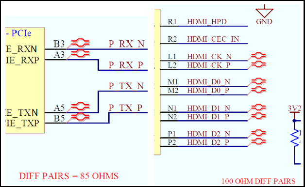
The design of a board starts with the design of the circuit schematics by the design engineer. The engineer must specify controlled impedance signals in the schematic and classify specific nets to be either differential pairs (100Ω, 90Ω or 85Ω) or single-ended nets (40Ω, 50Ω, 55Ω, 60 Ω or 75Ω). It’s a good design practice to add N or P polarity indication after the net names of the differential pair signals in a schematic. The engineer should also specify particular controlled impedance layout design guidelines (if any) to be followed by the layout designer, either in the schematic or in a separate “Read Me” file.
Determine the trace parameters for controlled CI
A PCB trace is defined by its thickness, height, width, and dielectric constant (Er) of the PCB material on which the traces are etched. While designing controlled impedance PCBs, it is essential to take care of these parameters. You can provide the manufacturer with the number of layers, the value of the impedance traces on specific layers (50Ω, 100Ω on layer 3), and materials for PCB designing.
The manufacturer gives you the stackup that mentions the trace widths on each layer, the number of layers, the thickness of each dielectric in the stackup, trace thickness, and PCB material. He also takes care of the controlled impedance requirements by calculating the feasible thickness, width, and height for the traces that need impedance control. Stick to the following relationships to know how impedance depends on dimensions:
- Impedance is inversely proportional to trace width and trace thickness.
- Impedance is proportional to the laminate height and it is inversely proportional to the square root of laminate’s dielectric constant (Er).