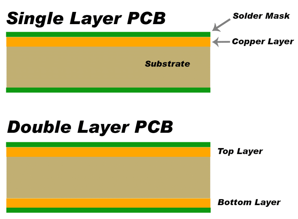
Layer Type and Advantages
The designer selects the layer number for the design according to the complexity of the entire circuit, which mainly considers two factors, the difficulty of the output lines of the core equipment and the layout of the equipment in the entire project.
#01.Single Layer
Single-sided PCB is mainly used in very simple consumer electronics products. After all, the process is simple. Now it uses cheap original circuit board materials (FR-1 or FR-2) and thin copper cladding. Single-panel circuit design often includes many jumpers to simulate circuit routing on double-sided boards.
Generally used more in low-frequency circuits. Because this type of design is easily affected by radiated noise. So designing this type of circuit board will be more troublesome, if not very careful, there will be many problems. Although there are successful cases in complex designs, they are things that need to be carefully considered and continuously verified.
Take an example, such as a TV, which places all analogue circuits on a single panel at the bottom of the case, and uses a metalized CRT to shield the circuit board on a separate digital tuning board near the top of the battery pack. If you need high-volume, low-cost PCB production, then you need to play it by yourself.
 #02.Double Layer
Equivalent to a single panel, a bit more complicated is the dual panel. Some double-layer panels are still made of FR-2, but FR-4 is more commonly used today. The increased strength of the FR-4 material better supports vias. Because there are two layers of foil, the dual-panel is easier to route, and signals can be planned by crossing traces on different layers. However, crossover traces are not recommended for analogue circuits. Where possible, the bottom layer is kept as complete as possible as a ground plane, and all other signals should be routed on the top layer. There are several benefits to the ground plane at the bottom:
- The ground is usually the most common connection in a circuit. The designer can connect all the GND networks on the whole board to the bottom layer.
- Increased mechanical strength of the circuit board.
- Reduce the impedance of all ground connections in the circuit, thereby reducing the conducted noise of the signal.
- Added distributed capacitance for each network in the circuit-helps to suppress radiated noise.
- Can shield radiated noise from under the circuit board.

Multilayer PCB
#03.Multilayer PCB
Despite its advantages, dual panels are not the best method of construction, especially for sensitive or high-speed circuit designs. Therefore, for high-speed designs, we usually use multi-layer boards for design. The most common board thickness is 1.6 mm, the material is FR-4, and there is an independent GND or POWER layer, etc. Many circuit design issues need us to notice in the multilayer board itself.
Below we have to clear some obvious reasons for using the multilayer board design:
- Have independent power and ground connection wiring layers. If the power supply is also on the same plane, simply adding vias can connect other identical power supply networks.
- You can use Other layers for signal routing, which can provide more routing space for wiring.
- Distribute capacitance between power and ground planes to reduce high-frequency noise.
However, other reasons for the multilayer board may not be obvious or intuitive, and there are two main points:
- Better EMI / RFI rejection. Due to the image plane effect, it has been known since the Marconi era. When you place a conductor close to a parallel conductive surface, most of the high-frequency current will return directly under the conductor and flow in the opposite direction. The mirror image of the conductor in the plane forms the transmission line. Since the current is equal and opposite in the transmission line, it is relatively unaffected by radiated noise. Instead, the signals are coupled very efficiently. Image plane effects are as effective as the ground and power planes, but they must be continuous. Any gaps or discontinuities will cause beneficial effects to disappear quickly.
- Reduce the overall project cost of small-batch production. Although multilayer boards are more expensive to manufacture, FCC or other agency EMI / RFI requirements may require costly testing of the design. If there is a problem, it may need to be pushed back to re-design the PCB for additional testing. Compared to a 2-layer PCB, the EMI / RFI performance of a multilayer PCB can be improved by 20 dB. If the yield is small, it makes sense to design a better PCB first.
- Effectively prevent crosstalk between various signal layers.
- The production process requirements are relatively high. Compared with the 2-layer board design, it is not so difficult.
