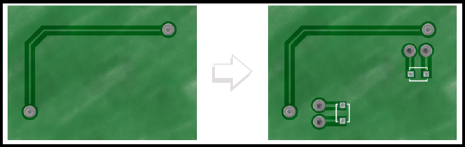
Differentiate CI traces from other traces
The controlled impedance trace widths must be distinguishable from the remaining traces on the board. It allows the PCB manufacturer to quickly identify them and make suitable changes to the trace width if necessary, to achieve a specific impedance. For example, if you require a 5mil trace to achieve 50Ω impedance and if you have also routed other signals with 5mils width, it will be impossible for the PCB manufacturer to determine which ones are the controlled impedance traces. Therefore, you should make the 50Ω impedance traces 5.1mils or 4.9mils wide.
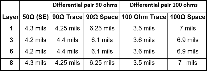
The table below shows trace widths and spacings for controlled impedance on different layers. Non-impedance signal traces should not be routed with 3.5, 3.6, 4.2, 4.25, and 4.3mil trace widths.
Maintain symmetry in differential pair routing
High-speed differential pair signal traces need to be routed parallel to each other with a constant spacing between them. The specific trace width and the spacing are required to calculate the particular differential impedance. The differential pairs need to be routed symmetrically. You should minimize areas where the specified spacing is enlarged due to pads or the ends.
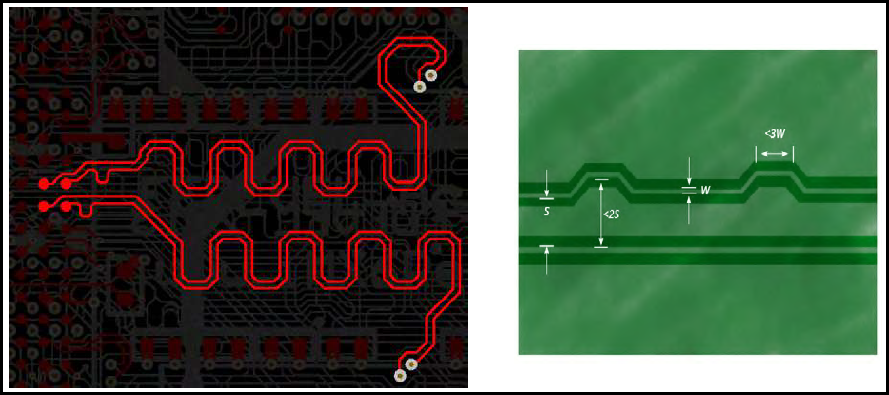
Adequate spacing b/w controlled impedance traces, other traces, and components (3W and 2W rule)
To reduce crosstalk, the spacing b/w traces should be 3W or at minimum 2W. Note that this rule does not apply to the spacing b/w differential pairs.
Placement of components, vias, and coupling capacitors
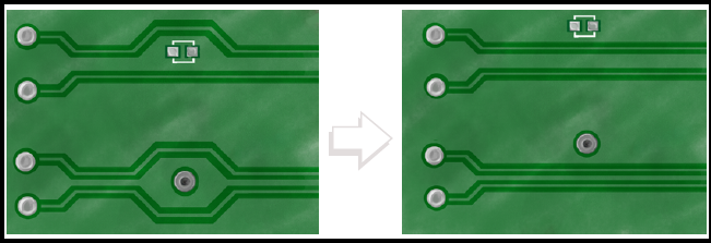
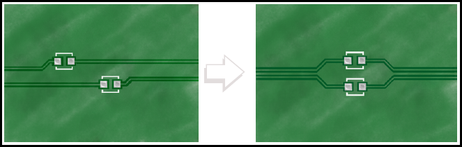
Components or vias should not be placed between differential pairs, even if the signals are routed symmetrically around them. Components and vias create a discontinuity in impedance and could lead to signal integrity problems. For high-speed signals, the spacing between one differential pair and an adjacent differential pair should not be less than five times the width of the trace (5W). You should also maintain a keep-out of 30mils to any other signals. For clocks or periodic signals, you should increase the keep-out to 50mils to ensure proper isolation.
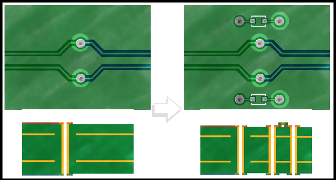
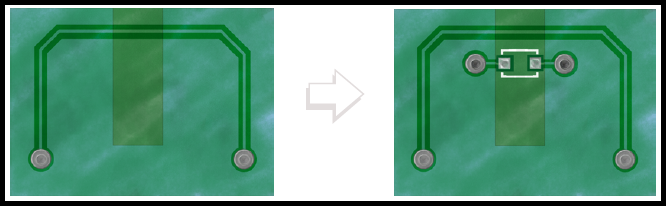
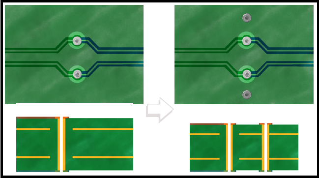
If high-speed differential pairs require serial coupling capacitors, they need to be placed symmetrically, as shown in the below figure. The caps create impedance discontinuities, so placing them symmetrically will reduce the amount of discontinuity in the signal.
You should minimize the use of vias for differential pairs, and if you do place them, they need to be symmetrical to minimize discontinuity.
Length matching
Length matching will achieve propagation delay matching if the speed of the signals on various traces is the same. Length matching may be required when a group of high-speed signals travel together and are expected to reach their destination simultaneously (within a specified mismatch tolerance).
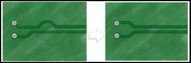
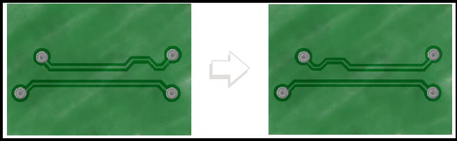
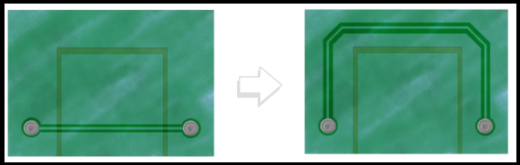
The lengths of the traces forming a differential pair need to be matched very closely; otherwise, that would lead to an unacceptable delay skew (mismatch between the positive and negative signals). The mismatch in length needs to be compensated by using serpentines in the shorter trace. The geometry of serpentine traces needs to be carefully chosen to reduce impedance discontinuity. The figure below shows the requirements for ideal serpentine traces.
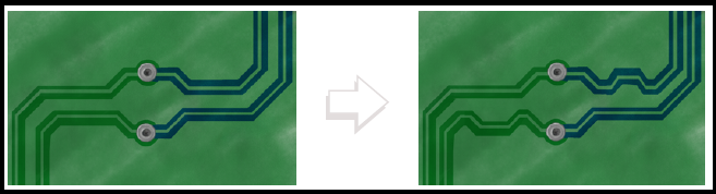
The serpentine traces should be placed as near as possible to the source of mismatch. It ensures the mismatch correction as soon as possible. In the figure below, you can see that the mismatch occurs on the left set of vias, so the serpentine needs to be added on the left rather than on the right.
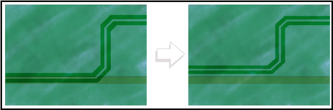
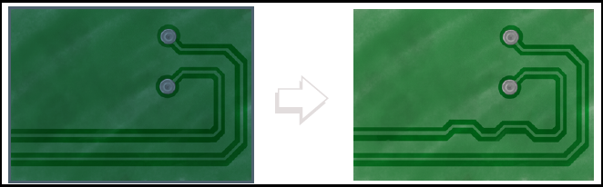
Similarly, bends cause mismatching making the trace on the inner bend smaller than the outer trace. Therefore, we need to add serpentines as close to the bend area. If a pair has two bends closer than 15mm, they compensate each other. Hence you do not need to add serpentines.
When a differential pair signal changes from one layer to another using vias and has a bend, each segment of the pair needs to be matched individually. Serpentines should be placed on the shorter traces near the bend. You need to manually inspect for this violation as it will not be caught in Design Rule Checks since the lengths of the total signals will be closely matched. Since the signal speed of traces on various layers may be different, it is recommended to route differential pair signals on the same layer if they require length matching.
Reference layers for the return path of controlled impedance signals
All high-speed signals require a continuous reference plane for the return path of the signal. An incorrect signal return path is one of the most common sources for noise coupling and EMI issues. The return current for high-speed signals closely follows the signal path, whereas the return current for low-speed signals takes the shortest path available. Generally, the return path for high-speed signals is provided in the reference planes nearest to the signal layer.
High-speed signals should not be routed over a split plane because the return path will not be able to follow the trace. You should route the trace around the split plane for better signal integrity. Also, make sure that the ground plane is a minimum of three times the trace width (3W rule) on each side.
If a signal needs to be routed over two different reference planes, a stitching capacitor between the two reference planes is required. The capacitor needs to be connected to the two reference planes and should be placed close to the signal path to keep the distance between the signal and the return path small. The capacitor allows the return current to travel from one reference plane to the other and minimizes impedance discontinuity. A good value for the stitching capacitor is between 10nF and 100nF.
You should avoid both split plane obstructions and slots in the reference plane just underneath the signal trace. If the slots are unavoidable, stitching vias should be used to minimize the issues created by the separated return path. Both pins of the capacitor should be connected to the ground layer and should be placed near the signal.
When vias are placed together, they create voids in reference planes. To minimize these large voids, you should stagger the vias to allow sufficient feed of the plane between vias. Staggering the vias allows the signal to have a continuous return path.
It is preferred to use ground planes for reference. However, if a power plane is used as a reference plane, you need to add a stitching capacitor to allow the signal to change the reference from the ground to the power plane and then back to the ground. You should place a capacitor close to the signal entry and exit points and connect one end to the ground and the other to the power net.
Add stitching vias close to the layer change vias.
If a high-speed differential pair or single-ended signal switches layers, you should add stitching vias close to the layer change vias. This practice also allows the return current to change ground planes.
If a high-speed signal trace switches to a layer with a different net as reference, stitching capacitors are required to allow the return current to flow from the ground plane through the stitching capacitor to the power plane. The placement of the capacitors should be symmetrical for differential pairs.