
Step 1: Inner layer core selection
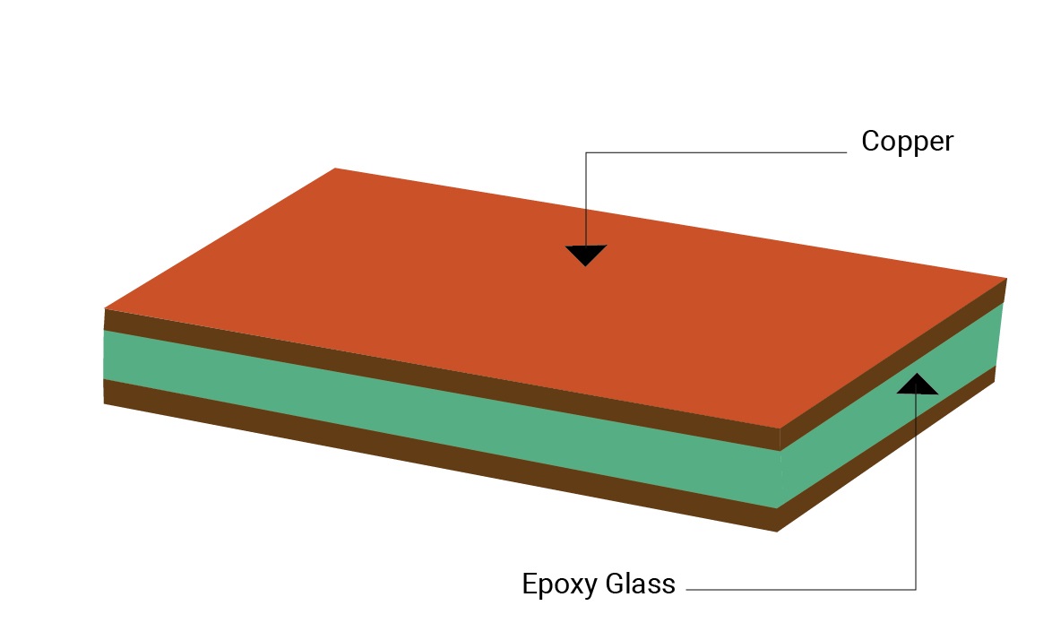
The stack-up designates the materials to be used for the manufacture of a multilayer circuit board. The build-up provides the following information:
- The copper thickness and weight
- Type of epoxy glass to be used
- Panel size
Step 2: Cleaning
The inner layers are cleaned chemically/mechanically or both to remove contaminants from the copper surface.
Step 3: Inner layer imaging
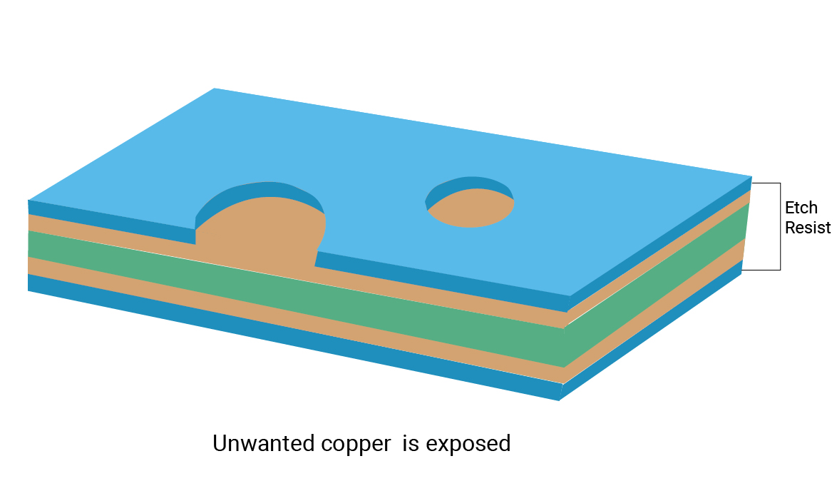
The imaging material is placed on the copper surface. It covers the desired copper circuitry and exposes the unwanted copper.
Step 4: Etch stripping
The inner layers are chemically etched to get rid of the unwanted copper. The photoresist is then stripped off to reveal the copper circuitry.
Step 5: Automated Optical Inspection
Automated optical inspection is carried out to find the flaws(shorts/opens in inner layers) that can’t be detected by the human eye.
Step 6: Oxide treatment
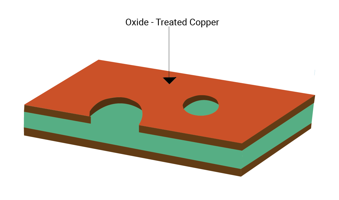
The exposed copper circuitry on the inner layer must be treated before lamination to improve adhesion. Improved adhesion also increases the structural strength and overall board reliability.
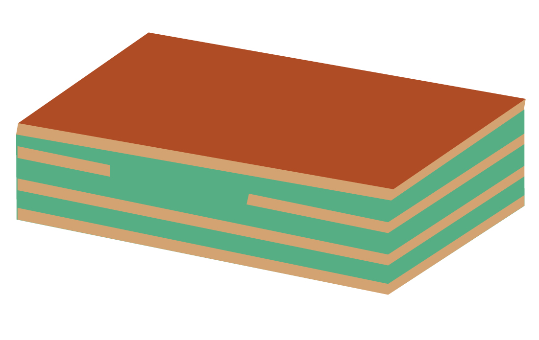
Step 7: Layup
Steps 1 to 6 are repeated for all the inner layers. For example, these steps will be carried for layers 2, 3, and 4, 5.
Step 8: Lamination
In this step, the stacks are pressed and heated in a vacuum chamber. The Lamination process begins by applying vacuum to remove all the entrapped air and gases. Later, heat and pressure are applied to the stack so the resin in the prepreg undergoes a molecular bonding.
Step 9: Drilling
After the lamination process, the laminated board is loaded on a panel of exit material on the drill bed. The holes are drilled on the PCB to make vias and through holes. The exit material lessens the burr formation. Burr is the protruding part of copper formed when the drill spindle penetrates through the board.
Step 10: Deburring and desmearing
In this step, the copper burrs formed during the drilling process are removed. It also removes any fingerprints on the copper surface. Desmearing is the process of removing friction-melted resin during the drilling process. The epoxy smear is removed by immersing the PCB panel in a series of chemical solutions followed by potassium permanganate or concentrated sulfuric acid. Desmearing can also be performed by plasma treating.
Step 11: Copper plating of drill holes
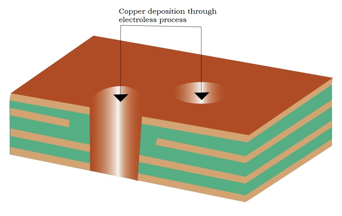
After deburring and desmearing, drill holes are copper plated using an electroless method.