
HDI board stack-ups
High-density interconnect, or HDI, circuit boards are printed circuit boards with a higher wiring density per unit area than traditional printed circuit boards. In general, HDI PCBs include microvias, blind vias, buried vias, built-up laminations, and high signal performance considerations.
Sequential lamination
PCBs are manufactured by layering an epoxy pre-impregnated fiberglass sheet between the copper layers. These layers are laminated together under high temperature and pressure. Sequential lamination is a process of inserting a dielectric between a copper layer and a laminated subset (laminated layers).
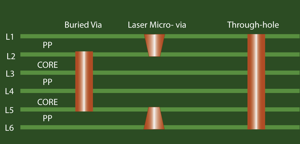
Buried vias can be built into HDI boards using a sequential lamination process. The first step is to fabricate the layers that are connected through a buried via (layers 2, 3, 4, and 5 in the given stack-up). Next, the outer layers (layers 1 and 6) are laminated and the microvia holes are drilled.
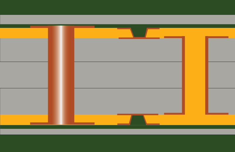
Now, let us assume that this design requires a connection between L1 & L3; L6 & L4. The best way to achieve this design is to use staggered or stacked vias as shown below.
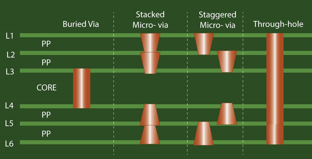
In the stack-up above, we can see that the micro-vias are stacked and staggered. Stacked vias are more space-efficient. However, they are less reliable and require complex manufacturing resulting in increased manufacturing price.
Staggered vias essentially mean fewer process steps. We do not have to fill the laser-drilled vias with copper because the second laser drill does not land on the first laser drill. Filling or plating a microvia shut usually happens in a special plating tank designed with chemistry. It plates the laser-drilled microvia from the bottom of the via to the top of the via, until it fills the hole completely. Plating a laser-drilled microvia shut adds time and cost to the process.
Nomenclature of HDI stack-ups
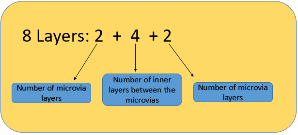
The HDI stack-up architecture is differentiated into stack-up classes depending on the number of microvia layers and the number of inner layers between the microvias. These classes are determined by formula X-N-X, where x is the number of microvia layers and N is the number of inner layers between the microvias.
Examples of HDI stack-up
1+4+1 STACK-UP
The above stack-up shows an example of a 6 layer stack-up(1+4+1) with one microvia layer on either side of the board.
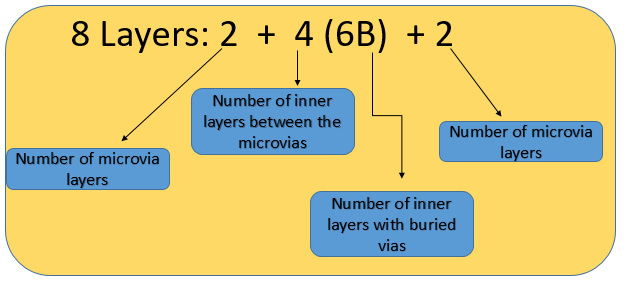
2+4(6B)+2 STACK-UP
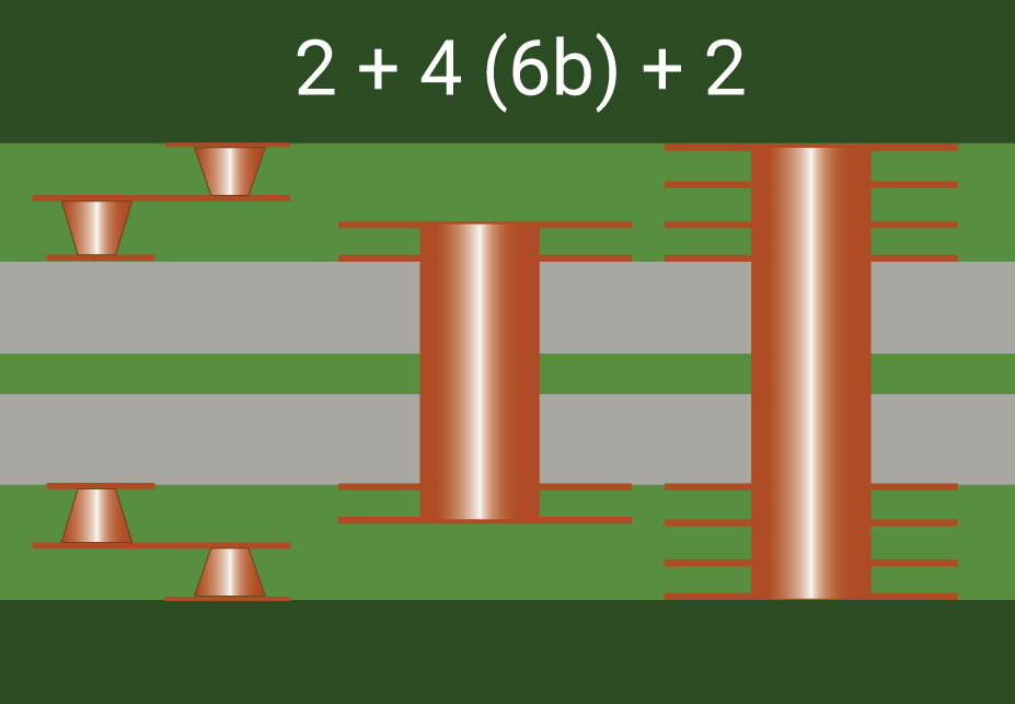
The above image shows an example of 8 layer stack-up with two microvia layers on either side of the board and 6 buried via layers between the microvia layers.