
1.Identifying thermal hotspots and high-current traces
To fabricate a thermally stable PCB, thermal effects must be studied during the designing phase itself. The first step in thermal design is to identify the hotspots. Thermal modeling or thermal simulation techniques are used to find hotspots. Also, current flow analysis must be done along with it, because high-current traces cause heat generation.
The proper geometrical arrangement of components and high-current traces enables even distribution of heat. High-current traces must be routed away from thermally sensitive components such as sensors and Op-amps.
2. Copper thickness and width of traces
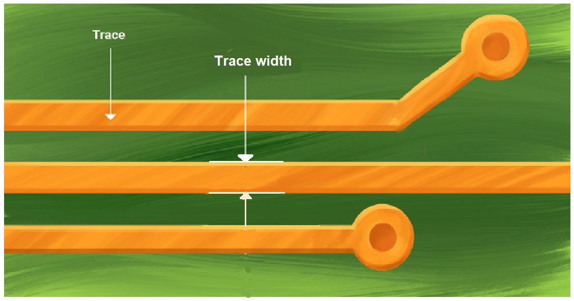
The thickness and width of the copper pad or traces play a significant role in PCB thermal design. Copper trace thickness should be adequate to provide a low impedance path for current passing through it. This is because the resistance of copper traces and vias accounts for significant power loss and heat generation particularly when they bear high current density. Therefore sufficient trace width and thickness are recommended to reduce heat generation.
3.Pad design for PCB thermal management
- Just like trace thickness, pad thickness is also important. Heat is dissipated directly towards the top copper layer. Therefore, the top copper pad must have sufficient thickness and area to provide enough heat spreading.
- If the PCB design has heat sinks in it, they are usually mounted on the bottom copper pad. Then the bottom copper pads should have sufficient coverage to allow optimum heat transfer to the heatsink.
- The component pins are soldered to the PCB supported by pads. The component is directly connected to the pad which results in very low thermal resistance to the PCB. A special welding pad that is thermal pads is used on the circuit board. This pad is only connected with thin bridges to the copper surrounding pour.
- The solder paste used to connect the component footprint with the thermal pad should be minimal. Too much solder paste under the thermal pads can result in the floating of components on a pool of molten solder during reflow. When this happens, the component package tends to move. The solution to the floating package problem is to optimize the solder paste volume.
4. Placing of high power components in PCB
For better heat dissipation, high power components such as processors and microcontrollers should be placed at the center of the PCB. If a high power component is mounted near to the edge of the board, it will accumulate heat at the edge and raise the local temperature. But if the device is placed at the center of the board, heat will scatter over the surface in all directions. Thus the surface temperature of the PCB would be lower and dissipates easily.
Also, make sure you have placed high-power components away from sensitive devices and keep the proper spacing between two high-power devices. Try to place high-power components evenly across the PCB.
5. PCB thermal vias design
Thermal vias are heat-conducting copper barrels that run between the top and bottom of the board. Such vias are good thermal conductors that transfer heat away from critical electronic components. These vias are typically used to facilitate rapid heat dissipation away from surface mount devices (SMD).
Suppose there is no space for a cooling system on top of the PCB, as in the case of an integrated sensor, indicator, or a packed board with numerous components. The simplest way to dissipate heat would be through thermal vias to the cooling system (heat sink or heat pipes).
Designers can use thermal vias for vertical heat transfer >between conductive layers. The number of thermal vias under BGAs or processors should be determined by the designers considering the heat dissipation range and surface area. Standard thermal via dimensions are as mentioned below:
- Diameter is 12 mil (0.3 mm) placed on 25 mils (0.64 mm) grid spacing.
- Standard copper plating thickness is 1 mil (25 μm)
- No via filling
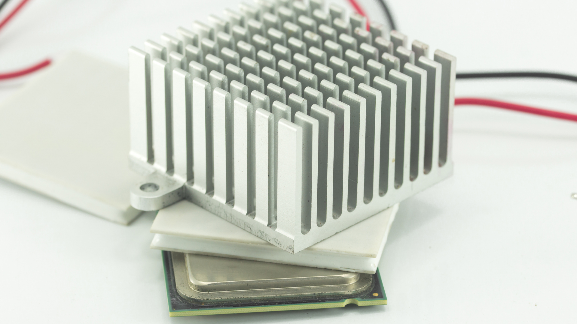
6. Heat sink
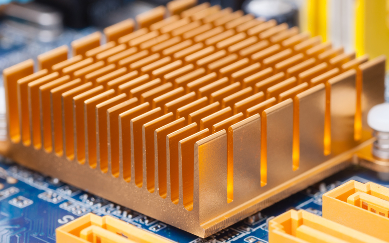
The heat sink is a cooling method that transfers dissipated heat from PCB components into a cooling medium. Heat sink works on the principle of conduction which states that heat transfers from an area of high thermal resistance to an area of low thermal resistance. The heat also flows from high-temperature areas to low-temperature areas and the amount of heat flow is directly proportional to the temperature difference. The heat sink draws heat away from the PCB to fins that provide a larger surface area for faster heat dissipation.
Designers can choose a suitable heat sink for their design based on several factors. For example, the thermal resistivity of material used, the velocity of cooling fluid inside the sink, the thermal interface material used, the number of fins and spacing between fins, the mounting technique used, etc.
7. Heat pipe integration
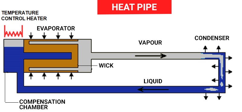
Heat pipes are cooling devices recommended for higher temperatures applications such as in rockets, satellites, and avionics. The heat pipes are mostly available in a hollow cylindrical shape, but it can be made into any shape conveniently.
Heat dissipated from various devices is transferred to the liquid inside the heat pipe and vaporizes the liquid. The vaporized liquid condensate at the condenser end and returns to the evaporator through the wick structure by capillary action. This cyclic process ensures the dissipated heat to flow away from the PCB.
Designers should consider a heat pipe that entirely covers their heat source and should be able to bend as per your design requirements. There is a wide range of heat pipe working fluids available, from cryogens to liquid metals. Working fluid selection depends on the temperature range of the circuit and the fluid’s chemical compatibility with the container and the wick of the heat pipe.
8. Thicker PCB boards
For smaller devices, cooling methods like a heat sink, heat pipes, cooling fans are not an option at all. In such cases, the only option is to increase the thermal conductivity of the board and spread the generated heat. Thick boards with a comparatively larger surface area can dissipate heat quickly.
The thermal conductivity of a PCB is determined based on the coefficient of thermal expansion (CTE) of the materials used and its thickness. Designers must give extra attention to choosing material for each layer in the PCB stackup. When the coefficient of thermal expansion of the various materials used in different layers is mismatched, upon repetitive thermal cycling, fatigue occurs to reduce the thermal conductivity. Copper plating in vias and solder balls are more vulnerable to damage under high thermal cycling.
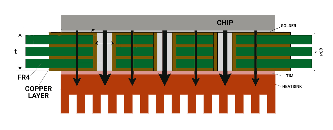
9. Integrated cooling methods
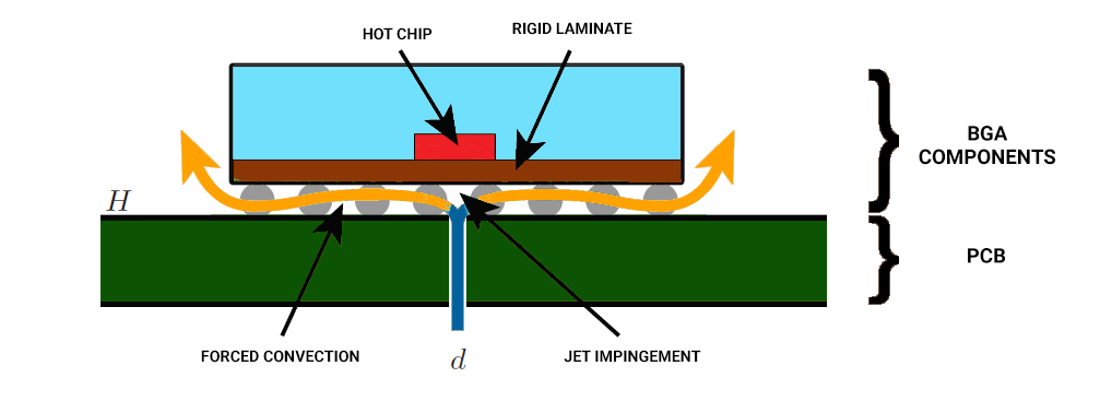
Integrated cooling methods are used to achieve higher coefficients of heat conductivity compared to a traditional heatsink & fan setups. The concept is to blow a cooling agent through dedicated vias directly to the bottom of the processors or BGAs or any heating components.
The number of vias should be determined by the designer, depending on the thermal criteria of the mounted component. A single via is considered first, more can be added on-demand which depends on the velocity of the cooling fluid, and the surface area of the component.
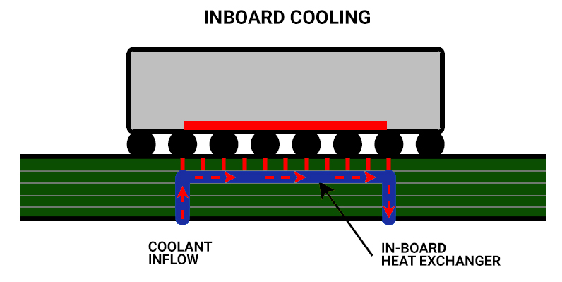
There are also other kinds of integrated cooling methods, for example, the inboard cooling method illustrated above. In this method, a heat exchanger is incorporated inside the board itself. Since no external heat sink or cold plate is required, the PCB assembly steps and the weight of the final product is reduced. But these coolers require a very high thermal via density around the cooling channels.
10. Cooling fans
We have gone through several cooling methods in this article, like heatsinks, heat pipes, thermal vias, etc. All these techniques exchange heat through conduction, which in many cases is not enough. The cooling fan uses convective heat transferring method that offers the designer a much efficient method for getting the heat away from components.
The efficiency of the fan depends on the ability to push a specific volume of air from the device and the compatibility of placing a fan. Designers must consider things like friction, size, noise, cost, operation, power requirement, etc while selecting the fan. But the fan’s primary purpose is to push a volume of air, which means capacity is the superior factor in choosing a cooling fan.
11. Soldering concentration
The soldering thickness of device joints should be even and ambient to reduce heat accumulation on the component leads. Extra care should be given while soldering near vias. There is a chance for the solder to overfill the hole leading to bumps on the bottom of the board and this reduces the contact area of the heat sink.
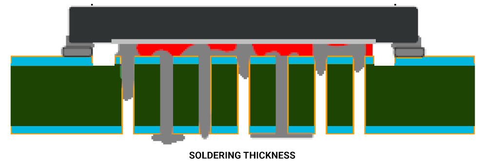
PCB designers have two options to avoid the overflow of solder. The first one is to decrease the diameter of the via below 0.3mm. The smaller the vias, the surface tension of the liquid solder inside the via is better able to counter the force of gravity on the solder.
The second option is the process called tenting. It involves covering the pad of the via with a solder mask to prevent the solder from flowing down to the via.
12. Peltier heat pump / Thermoelectric coolers (TEC)
Time to upgrade to advanced techniques in PCB cooling. Thermoelectric cooling or Peltier heat pump methods use the Peltier effect for cooling. Peltier effect is the reverse of the generation of thermal steam. These devices can cool components to sub-ambient temperatures.
TECs are used where the component temperature should be kept at a particular level. For example CCD cameras (charge-coupled devices), laser diodes, microprocessors, night-vision systems, etc. TECs offer accurate temperature control and faster response. Designers can use a combination of TECs with air cooling or liquid cooling techniques to extend the conventional air cooling limits for high-power dissipating processors. Commercial Peltier pumps cover a range of ceramic face sizes from 3.2 × 3.2mm² to 62 × 62mm² at the cooling side, from 3.8 × 3.8mm² to 62 × 62mm² at the base (heated side).