PCB HERO Manufacturing Capabilities: PCB/Assembly in 2021
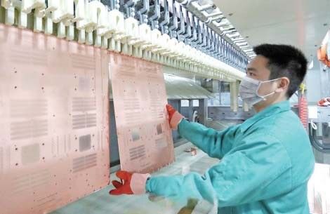
PCB HERO is an advanced PCB manufacturer founded in 1999. Over the 22 years, we had built three PCB and PCBA manufacturing bases - one PCB factory in Jiangxi, one PCB factory in Jiangsu, and one PCB assembly factory in Shenzhen. All levels of production, from prototypes to large-scale manufacturing, happen on the same production lines. You may be curious - what are the manufacturing capabilities of PCB HERO?

First, let's look into the PCB manufacturing capability. We focus on high-end PCBs, such as the flexible (FPC), rigid-flex PCB, HDI, etc. And below is our capabilities:
PCB Technical Capacity
We classify the printed circuit boards into the HDI board and plated through-hole boards. Here are our PCB manufacturing capabilities.
|
Technical Capabilities
|
HDI PCB
|
Plated Though-Hole Boards
|
|
Maximum Layers
|
24
|
24
|
|
HDI Stackup
|
3+N+3
|
/
|
|
Max. Processing Board Size
|
24.5" × 28.5" (620 × 720mm)
|
24.5" × 37.5" (620mm × 950mm)
|
|
Min. Line Width/Line Space
|
I/L: 2.5mil/2.5mil O/L: 4mil/4mil (POFV)
|
I/L: 2.5mil/2.5mil O/L: 4mil/4mil(POFV)
|
|
Board Thickness
|
3.5mm
|
4.0mm
|
|
Min. Drill Bit
|
6mil
|
6mil
|
|
Aspect Ratio
|
18:01
|
18:01
|
|
Min. Micro Via & Aspect Ratio
|
4mil & 0.8:1
|
/
|
|
Min Core Board Thickness
|
2mil
|
2mil
|
|
Alignment between Layers
|
5mil
|
5mil
|
|
Solder Mask Tolerance
|
±8%
|
±8%
|
|
Back Drill stub
|
2-10mil
|
2-10mil
|
|
Copper Fill
|
Yes
|
/
|
|
POFV
|
Yes
|
Yes
|
|
Skip-via (L1-3)
|
No
|
No
|
|
Buried Copper Block
|
Yes
|
Yes
|
|
Buried Capacitance
|
No
|
No
|
Please note that plated through-hole PCBs in our chart includes many types of PCBs, such as high-frequency, ceramic, thick-copper, high-TG, halogen-free, etc. I will add the specific specifications charts of these advanced boards to this post when I am done. Let's see PCB HERO's capabilities of flexible PCB (FPC) and rigid-flex PCB.
FPC and Rigid-Flex PCB Capabilities
|
Technical Capabilities
|
Flexible PCB
|
Rigid-Flex PCB
|
|
Maximum Layers
|
6
|
10
|
|
Min. Mechanical Drilling Hole Diameter
|
0.1mm
|
0.15mm
|
|
Min. Laser Blind Hole Aperture
|
0.075mm
|
0.1mm
|
|
Max. Blind Hole Aspect Ratio
|
0.8
|
1
|
|
Blind Hole Buried Copper
|
No
|
Yes
|
|
Min. Through-Hole Pad
|
0.3mm
|
0.35mm
|
|
Min. Blind Hole Capture/Login Pad
|
0.275mm
|
0.25mm
|
|
Minimum Line Width/Line Space
|
0.035/0.035mm
|
0.065/0.065mm (rigid board layer)
|
|
Min. Interlayer Alignment
|
±0.05mm
|
±0.05mm
|
|
Min. Hard Board Dielectric Layer Thickness
|
/
|
±0.05mm
|
|
Surface Finishes
|
ENIG, OSP, ENEPIG, Immersion Tin
|
|
Applications
|
display module, smartphone, camera module, consumer electronics
|
PCB HERO's target customers are senior engineers and electronic solutions companies. If you are looking for a long-term PCB manufacturer for your devices, contact us by email at :nancy@pcb-hero.com.
PCB Assembly Capabilities
PCB HERO has mature SMT, THT, DIP lines for advanced PCB assembly. Our one-to-one engineering support, BOM and component inspection, and first piece test will make sure the assembly's success.
The below image shows the functional mounting machine we use in our assembly factory. Functional mounting machines are used to mount components of big sizes, such as BGA, FPGA, etc. Its capabilities can stand for part of our assembly capabilities:

|
Specifications
|
Values
|
|
Placement Accuracy
|
±0.035mm (Cpk≥1)
|
|
Placement Speed
|
42,000CPH
|
|
Feeder Inputs
|
Max. 112
|
|
Min. Board Size
|
50mm * 50mm
|
|
Max. Board Size
|
1,200mm * 370mm
|
|
Max. Rectangular Part Size
|
50mm * 150mm
|
|
Max. Square Part Size
|
74mm * 74mm
|
|
Max. Component Height
|
25mm
|
|
PCB Thickness
|
0.3mm - 4.0mm
|
|
Min. Component Size
|
0201mm
|
No matter what the circuit board quantity is, our manufacturing standards and procedures are the same. We never reduce PCB quality. Our strong manufacturing capabilities can meet all your requirements. If you have not been worked with PCB HERO, welcome to get a quote online or contact us. Our circuit board quality will meet and exceed your expectations.
