
How to Prevent Acid Traps
An acid trap is an area of a PCB that holds corrosive chemicals that should be washed away. Acid traps can be hard to detect, even for those experienced in PCBs. Many designers fall victim to them.
Defending against them isn’t a particularly difficult task, and it’s much easier to do than to fix the effects of acid corrosion. A little basic preparation and care can help your company keep designs free of acid traps and the damage they bring.
1. Ensure Your Design Is Flawless
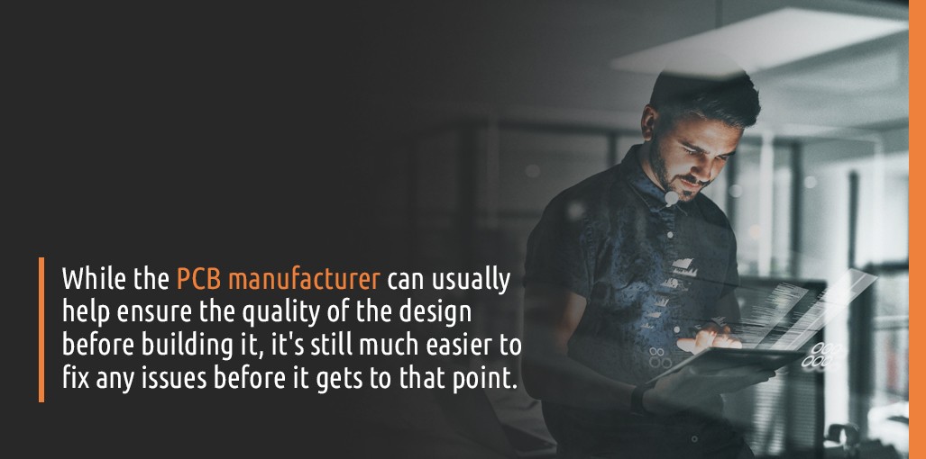
While the PCB manufacturer can usually help ensure the quality of the design before building it, it’s still much easier to fix any issues before it gets to that point. Review the circuit board’s layout carefully and look for acute angles and trace gaps that could create pockets for the acid to collect in. There shouldn’t be any places that could cause problems down the road.
The manufacturer will sometimes run a design through software that tests it for its manufacturability, so they know that the PCB’s layout won’t lead to problems. It may also help to identify PCB design issues that a DRC can’t catch. Your company can also perform this step if you want to be more prepared.
2. Drill More Holes With Extra Vias
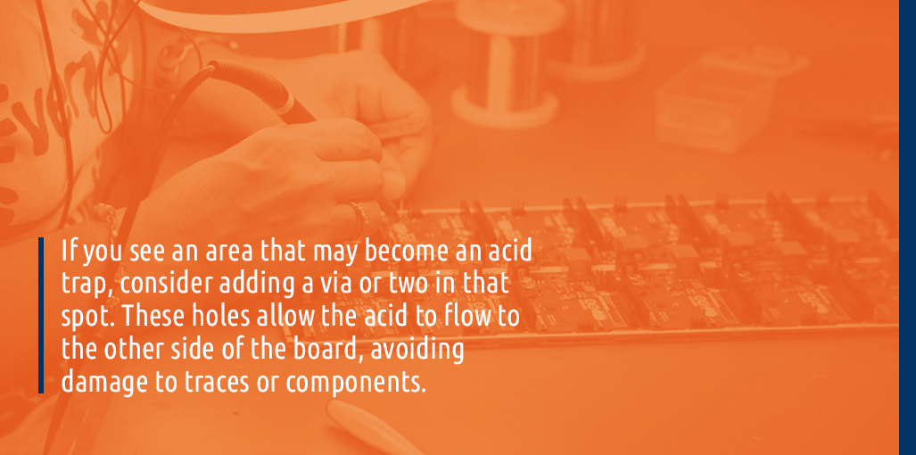
If you see an area that may become an acid trap, consider adding a via or two in that spot. These holes allow the acid to flow to the other side of the board, avoiding damage to traces or components. Of course, this requires caution, so you don’t drill through anything important on either side. Double-layered boards can be tricky in this regard, and this approach is best for single-sided boards.
Watch out for the hazards of group vias. When placing multiple vias close to traces, they can create pockets that become acid traps. Make sure that your design keeps gaps in between vias to space them further apart. They shouldn’t be close to each other or traces. The small amount of board real estate available in PCB design can make this spacing difficult. So increase the gaps if possible.
3. Use Photoactivated Etchants
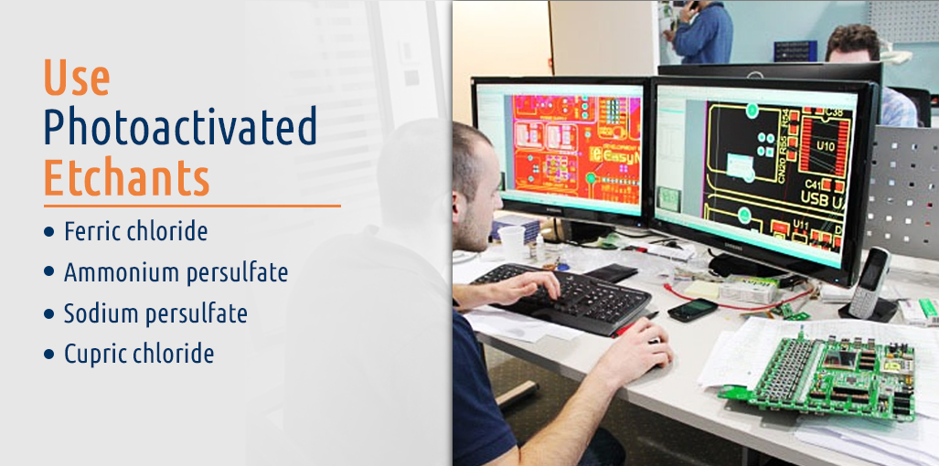
Using photoactivated etchants is one of the easiest and simplest ways to avoid acid traps, and most PCB manufacturers are jumping on this route. It eliminates many of the hazards of acid traps. Traditional etching chemicals include:
- Ferric chloride
- Ammonium persulfate
- Sodium persulfate
- Cupric chloride
The modern approach of using photosensitive films offers many benefits over their predecessors. Though you still need to abide by the PCB etching process, you can minimize the impact of overaggressive chemicals by using the photosensitive approach. Most PCB manufacturers now use more modern procedures that eliminate the use of corrosive materials like ferric chloride and hydrochloric acid. When you use these chemicals, there may be a higher chance of the acid seeping into unwanted areas and corroding more copper. Eliminating these chemicals all together is a great way to avoid their destructive effects.
Photoactivated etchants are those that activate or harden underneath a UV light. They aren’t very reactive unless exposed to the right type of lighting. If the etchant is in a blocked-off area of the board, the lack of light prevents it from causing too much damage. Even thicker layers of copper perform well with photoactivated etchants. They offer cleaner edges and can, therefore, help reduce acid collection in certain areas. These etchants also tend to be less corrosive, so if they become trapped in corners and pockets, they won’t affect the copper as much as traditional chemicals. This method is the one commonly used today as it tends to offer better results.
Working with a fabricator that uses photosensitive films is one of the most significant ways to reduce the risk of acid traps. This chemical aggressiveness is more of an issue for DIY PCB builders, but businesses that operate on larger scales shouldn’t have a problem finding manufacturers that work with modern materials.
4. Run DRC
This step may seem like a no-brainer, but running DRC before submitting a design is a critical step. This software will help you identify issues present on your board. It analyzes your layout against a set of defined parameters to see whether or not the board has those parameters in place. For instance, you can use DRC to check that your trace lines meet a specified width and whether circuits have separate grounds. You can also use it to check that all your angles are properly sized, and there aren’t any small gaps. The DRC step is especially vital if your board is high-density or has multiple layers.
5. Run DFM and Use Modern Manufacturing Methods

Design for manufacturing (DFM) software is an excellent way to check your board for its manufacturability. It improves the ease and efficiency of the manufacturing process, and that includes how it is going to stand up to the etching process. Acid traps, after all, occur during manufacturing. It can also help optimize a board in terms of dimensions and materials, making life a little easier for everyone involved. Running a design through a DFM program can help identify acid trap issues before they cause problems.
Another manufacturing consideration involves the modernity of your manufacturer’s process. Using photosensitive chemicals is one indicator of their practices. Learn about their manufacturing technique and assess whether it works for your needs. PCB design has come a long way, so make sure your manufacturer has kept up with the times.
5. Double Check Your Work
Even running DRC can’t catch everything. Plus, human errors are common. Like spellcheck, you can’t depend on the DRC to find all errors in your work. Go over your design carefully, looking out for any of the pitfalls we’ve mentioned. It may be an extra step, but spending a little more time and effort here can offer significant savings in fixing errors and defective PCBs. It may even help to have another designer take a look to get a second pair of eyes.
Catching acid traps before your board reaches the manufacturing stage is crucial to minimizing wasted operational costs and getting boards printed on schedule. If circuit boards get printed with acid traps in place, you end up with a bunch of defective boards. Taking steps to eliminate acid traps before they reach manufacturing can save you a lot of headaches down the road and make the process smoother for both your company and the manufacturer.