
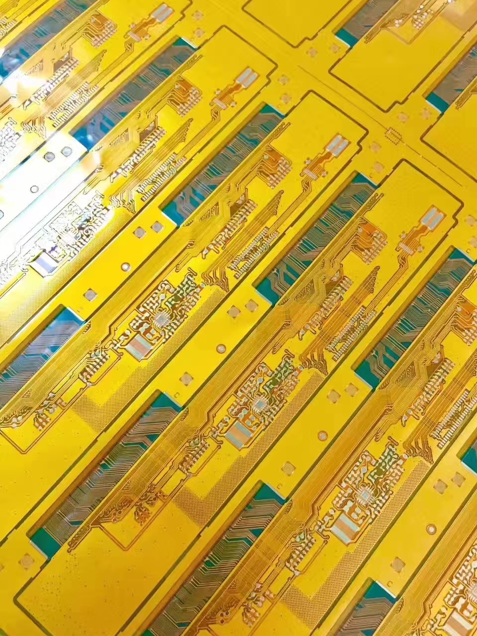
Blind Vias Flexible PCB
Blind vias are a type of via used in printed circuit board (PCB) design and manufacturing. They differ from traditional through-hole vias because they do not extend through the entire PCB.
Instead, they only go through one layer of the PCB and are often used to connect the inner layers of a multilayer PCB without breaking through to the opposite side of the board. This can be useful for reducing the overall size of the PCB and for hiding the vias from view.
Blind vias are often used in flexible PCBs, which are PCBs that are made from flexible, bendable materials such as polyimide. Flexible PCBs are helpful in various applications, including in electronic devices where the PCB needs to be adjustable to fit into a particular shape or be able to move or bend.
One challenge in using blind vias in flexible PCBs is that the vias must withstand the stress and strain of the bent or flexed PCB. This requires careful design and manufacturing of the vias, as well as the use of strong and flexible materials to withstand the forces applied to the PCB.
One way to increase the strength and flexibility of blind vias in flexible PCBs is to use laser drilling to create the vias. Laser drilling is a precise, high-tech method of creating small holes in a PCB, and it can be used to create blind vias with very small diameters and high aspect ratios (the ratio of the depth of the via to its diameter).
Another option is to use flexible materials for the via fills, which can help to reduce the stress on the vias when the PCB is bent or flexed. For example, a flexible resin or conductive ink can be used to fill the vias, which can help to distribute the stresses more evenly throughout the via and reduce the risk of the via breaking or becoming damaged.
Buried Via Flexible Pcb
Buried via flexible printed circuit boards, also known as BVFPCBs, are a type of flexible circuit board with vias (conductor pathways) buried within the layers of the board. These vias are not visible from the board's surface and are typically used to connect different circuit board layers.
One of the main benefits of using BVFPCBs is their ability to improve a circuit board's overall reliability and performance.
Since the vias are buried within the layers of the board, they are protected from external damage and are less likely to experience issues such as short circuits or breaks in the circuit.
This makes them ideal for use in harsh environments or applications where the circuit board may be subject to physical stress or exposure to contaminants.
In addition to their reliability, BVFPCBs also offer several other advantages. They are more flexible than traditional circuit boards, which makes them easier to bend and shape to fit into tight spaces or conform to curved surfaces.
This can be especially useful in applications where the circuit board needs to be flexible or conform to a specific shape.
BVFPCBs are also lightweight and thin, making them ideal for portable or compact electronic devices. They are also more cost effective than traditional circuit boards, requiring fewer layers and less material to manufacture.
Overall, buried via flexible printed circuit boards are a highly reliable and versatile option for a wide range of electronic applications. They offer improved performance, flexibility, and cost savings, making them an attractive choice for manufacturers and designers.
Blind And Buried Vias Flexible PCB
Blind and buried vias are interconnects used in flexible printed circuit boards (PCBs). These vias are not visible on the top or bottom surfaces of the PCB and are instead buried within the layers of the board. This allows for a more compact design, increased routing density, and improved signal integrity.
One of the main advantages of using blind and buried vias in flexible PCBs is their ability to provide increased routing density. This means that more components can be placed on the board, making it possible to create smaller, more compact devices.
Additionally, using blind and buried vias can help to improve signal integrity by reducing the distance that signals travel, resulting in better performance and more reliable operation.
However, some challenges are associated with using blind and buried vias in flexible PCBs. One of the main challenges is that these vias are more difficult to manufacture, as they require specialized equipment and processes.
Additionally, the use of blind and buried vias may increase the cost of the PCB, as they are more expensive to produce than other types of interconnects.
Despite these challenges, the benefits of using blind and buried vias in flexible PCBs often outweigh the costs.
These vias allow for more compact designs, increased routing density, and improved signal integrity, all critical factors in the design and performance of modern electronic devices. As such, they are likely to continue to be an important part of the flexible PCB industry in the coming years.
Blind Via Flexible PCB Stackup
A flexible PCB stackup is the arrangement of layers in a flexible PCB. These layers can include conductive, dielectric, and adhesive layers and blind vias for interconnections. The stackup is important for determining the overall performance and reliability of the PCB.
One of the key benefits of using blind vias in a flexible PCB stackup is their ability to reduce the number of layers required. This is because the vias can interconnect layers that are not visible on the surface, allowing for a more compact design. This can also help to reduce the overall cost of the PCB, as fewer layers mean less material and labor required.
Another advantage of using blind vias in a flexible PCB stackup is their ability to improve the flexibility of the PCB. By using blind vias to interconnect layers, the PCB can be more easily bent and flexed without damaging the connections. This can be especially important in applications where the PCB will be subjected to stress or movement, such as in wearable or medical devices.
There are a few considerations to keep in mind when using blind vias in a flexible PCB stackup. One of these is the size of the vias, as larger vias may be more prone to failure or damage when the PCB is flexed. It is also important to carefully plan the routing of the vias to ensure they do not interfere with other components or structures on the PCB.
Overall, blind vias are a useful tool for designing flexible PCBs, allowing for a more compact and flexible stackup. They can reduce the number of layers required and improve the flexibility of the PCB, making them a valuable consideration for any design engineer.
Blind Via Flexible PCB Material
Blind Via Flexible PCB material is a printed circuit board used to manufacture electronic devices. This type of PCB is made using a flexible material such as polyimide or polyester, which allows it to be bent or flexed without damaging the circuitry.
One of the main advantages of using a Blind Via Flexible PCB is its ability to be used in many applications. This type of PCB is often used in devices that need to be portable or have a small form factor, such as smartphones, tablets, and wearable devices. It is also used in medical devices, military equipment, and aerospace systems.
One of the key features of a Blind Via Flexible PCB is its ability to connect different layers of the circuit board without the need for through-hole vias. This is known as a "blind via," and it allows for more efficient and compact circuit board design. This is especially useful in devices with multiple layers of circuitry, as it reduces the amount of space required for the vias and allows for more complex designs.
Another advantage of Blind Via Flexible PCBs is their improved performance and reliability. Because the vias are not exposed to the surface of the circuit board, they are less prone to damage and failure. This makes them ideal for use in applications where durability and reliability are critical, such as in military and aerospace systems.
In addition to their functional benefits, Blind Via Flexible PCBs also offer several manufacturing advantages. They are easier to manufacture than traditional PCBs, requiring fewer steps and materials. This makes them more cost-effective to produce and allows for faster turnaround times.
Blind Via Flexible PCBs are a versatile and reliable option for electronic device manufacturers. They offer a range of benefits, including improved performance, compact design, and cost-effectiveness, making them an ideal choice for a wide range of applications.
Blind Buried Vias Flexible PCB Via In Pad Fabrication Process
Blind buried vias are a type of via used in flexible printed circuit board (PCB) manufacturing. They are called "blind" because they do not go all the way through the PCB and are "buried" because they are hidden beneath the surface layers of the PCB.
This allows for a more compact design and more space on the surface for components and other features. The "via in pad" fabrication process refers to placing these vias within the pads (or areas designated for components) on the PCB.
There are several steps involved in the blind, buried vias flexible PCB via in-pad fabrication process:
1. Design and Layout
The design and layout phase of the blind, buried vias flexible PCB via the in-pad fabrication process is crucial in ensuring the final product meets the desired specifications and functions properly. During this phase, a detailed plan is created for the circuit board, including the placement of all components, traces, and vias. The design should consider the PCB's flexibility and the board's desired final shape and size.
Once the design is complete, it is important to carefully review and verify it to ensure that all components are placed correctly and that the trace routing is efficient and free of errors. Any errors or inconsistencies discovered during this phase can be corrected before moving on to the next steps in the fabrication process.
The design and layout phase also involves creating a photolithographic mask, a negative image of the circuit board that will be used to transfer the design onto the PCB material. The mask is created by exposing a light-sensitive film to UV light through a patterned mask, which causes the film to harden in certain areas. The accuracy of the photolithographic mask is critical in ensuring that the final PCB accurately reflects the design.
Overall, the design and layout phase is a critical step in the blind, buried vias flexible PCB via the in-pad fabrication process, as it sets the foundation for the rest of the process and determines the outcome of the product. Ensuring a complete and accurate design and layout can save time and resources in the long run and result in a high-quality, functional PCB.
2. Etching
The etching process involves removing unwanted material from the PCB using a chemical etchant. This is done to create the desired circuit patterns and features on the PCB.
Etching is a crucial step in the blind, buried vias flexible PCB via the in-pad fabrication process, as it involves creating the vias themselves. This process uses two main methods: chemical etching and laser drilling.
Chemical etching involves immersing the PCB in a solution that removes the copper in the areas defined by the etch mask, creating the vias. This process is typically used to create larger vias and requires careful control of the etching solution and the amount of time the PCB is immersed.
Laser drilling creates smaller, more precise vias and is typically used in conjunction with chemical etching. In this process, a high-energy laser beam is used to create small holes in the PCB, which are then enlarged and connected using the chemical etching process. Laser drilling is a precise and efficient method for creating small vias, but it can be more expensive than chemical etching.
Regardless of the method used, etching requires careful attention to detail and precise execution to ensure proper connections and performance. Any errors or defects in the etching process can affect the overall performance of the PCB and may require rework to correct.
3. Via Formation
The formation of vias in a flexible printed circuit board (PCB) is an important step in the via-in-pad fabrication process. Vias are small holes that allow connections between different layers of the PCB and are typically filled with a conductive material to ensure proper electrical conductivity.
In the case of blind buried vias, these holes are not drilled through the PCB but are only accessible from one side. Forming these vias involves drilling through the PCB and filling the holes with a conductive material.
Several methods can be used to drill the vias, including mechanical drilling, laser drilling, and chemical etching.
Mechanical drilling involves using a physical tool, such as a drill bit, to create holes in the PCB. This method is typically used for larger vias or when precise control is unnecessary.
Laser drilling involves using a focused beam of light to vaporize the material in the PCB, creating a small, precise hole. This method is typically used for smaller vias or when higher levels of accuracy are required.
Chemical etching involves immersing the PCB in a solution that etches away the material in the PCB, creating a hole. This method is typically used for larger vias or when precise control is unnecessary.
Once the vias have been drilled, they are filled with a conductive material. This can be done using electroplating, where a thin layer of conductive material is deposited onto the surface of the PCB.
The PCB is then heated to cure the conductive material and ensure proper adhesion. Other methods of filling the vias, such as conductive polymer filling, may also be used depending on the requirements of the PCB.
Overall, forming vias in a flexible PCB is critical in the via-in-pad fabrication process. Properly formed vias are essential for ensuring proper electrical conductivity and connection between different layers of the PCB.
4. Surface Mount Technology
Surface mount technology (SMT) is a way to make electronic circuits where the parts are attached to the surface of the printed circuit board (PCB) instead of being put into holes.
This technology has revolutionized the electronics industry, allowing smaller and more complex circuits to be produced at a lower cost.
In the SMT process, the components are placed onto the PCB using a pick-and-place machine, which is a machine that is specifically designed to position the components onto the PCB accurately.
The components are typically held in place using a sticky adhesive, keeping them in place while being soldered.
After the components have been placed onto the PCB, the next step is to solder them. This is typically done using a reflow oven, which uses heat to melt the solder, bonding the components to the PCB.
The reflow oven has a series of temperature zones that are carefully controlled to ensure that the solder is melted at the correct temperature and for the correct amount of time.
One of the main advantages of SMT is that it allows for smaller and more complex circuits to be produced; because the components are mounted directly onto the surface of the PCB, they do not need to be inserted into holes, which means that the PCB can be made much smaller.
This is particularly useful for applications where space is at a premium, such as smartphones or other portable electronic devices.
SMT is also faster and more efficient than traditional manufacturing methods. Because the components are placed onto the PCB using a machine, the process is much faster and more accurate than manual assembly. This results in a higher yield and lower production costs.
Overall, surface mount technology has significantly impacted the electronics industry, allowing smaller and more complex circuits to be produced at a lower cost and in less time.
It is an essential technology in the modern electronics industry and is used in various applications, from smartphones and laptops to medical devices and industrial equipment.
5. Clean PCB
After the vias have been created and filled with a conductive material, it is important to clean the PCB to remove any residue from the etching and filling processes. This step is crucial for ensuring that the PCB is ready for testing and final inspection.
If any residue is left on the PCB, it can interfere with the connections and functionality of the vias, leading to performance issues.
Several methods can be used to clean the PCB, including manual, ultrasonic, and chemical cleaning. Manual cleaning involves using a soft cloth or brushes to remove any residue from the surface of the PCB gently.
Ultrasonic cleaning involves immersing the PCB in a solution and using ultrasonic waves to remove any particles or debris. Chemical cleaning involves using specialized cleaning agents to remove any residue from the PCB.
It is important to choose the appropriate cleaning method based on the specific needs of the PCB. For example, manual or ultrasonic cleaning may be more appropriate if the PCB has delicate components or good features.
If the PCB has stubborn residues that are difficult to remove, chemical cleaning may be necessary.
Regardless of the cleaning method chosen, it is important to follow proper procedures and take appropriate safety precautions to prevent damage to the PCB or harm to oneself.
This may include wearing protective equipment, such as gloves and eye protection, and following the manufacturer's instructions for the cleaning agents.
Cleaning the PCB is an important step in the blind, buried vias flexible PCB via the in-pad fabrication process. It helps to remove any residue from the etching and filling processes and ensures that the PCB is ready for testing and final inspection.
Choosing the appropriate cleaning method and following proper procedures and safety precautions are crucial for ensuring the integrity and performance of the PCB.
6. Test Connections
Testing the connections and functionality of the vias in a flexible printed circuit board (PCB) is an important step in the via-in-pad fabrication process.
This step helps to ensure that the vias are properly connected and functioning as intended, which is essential for the overall performance of the PCB.
Several methods can be used to test the connections and functionality of the vias, including visual inspection, electrical testing, and functional testing.
Visual inspection is a simple but effective method for checking the connections and functionality of the vias. This involves examining the PCB under a microscope or other magnifying device to look for any visible defects or issues with the vias.
This can include checking for proper alignment, ensuring that the vias are filled with conductive material, and looking for any signs of damage or defects.
Electrical testing involves using specialized equipment to test the electrical properties of the vias. This can include measuring the resistance of the vias, checking for continuity between different layers of the PCB, and verifying that the vias are properly connected to the circuits on the PCB.
This type of testing is typically done using automated testing equipment that can quickly and accurately measure the electrical properties of the vias.
Functional testing involves using the PCB in a real-world application to ensure it functions properly. This can include testing the PCB in a circuit or device or running software simulations to ensure the vias work correctly in different scenarios.
This type of testing can help to identify any issues with the vias that may not be visible during visual inspection or electrical testing.
Overall, testing the connections and functionality of the vias is an essential step in the blind, buried vias flexible PCB via the in-pad fabrication process.
By using a combination of visual inspection, electrical testing, and functional testing, manufacturers can ensure that the vias are properly connected and functioning as intended, which is essential for the overall performance and reliability of the PCB.