
We are quick to forget how technological advancements have contributed to our existence. A brief flashback will be helpful to appreciate these developments at our disposal. The USB adds up to one of such developments.
The USB world is a vast grassy field of interface. It has provided solutions to sharing of files, transfer of data, images and programs. Also, it is an interface between USB and various computing, electronics and communication devices. It has grown over time as a technology that has become customary to tasks and play devices.
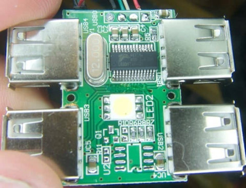
There are various types of connectors roving around the field of PCB production. They show the means by which power relays data transfer as input to producing new outputs. These interfaces are in two gender form, the male and female
In a bid to please curiosity on what the new technology in appliances for both tasks and play provides, read on. This article will explore PCB USB, USB PCB connector, USB c PCB, USB circuit board, and others.
What is PCB USB?
The abbreviation USB means Universal Serial Bus. This is basically a snap-in device that plays the role of an interface between PCB and its subsidiaries. Its expansion has been very huge and its dominance well felt in the technological world. Its relevance and contribution to the world economy today as well is significant.
It is self reliant without dependence on any device to run, or the need to charge for power before use. Its efficiency has helped businesses and corporations transfer document cases with relative ease.
The PCB USB is a sought after connecting found in various electronic devices. They include computers, mobile phones, pen drives, printers and many more. It aids initiating connections with accomplices. The USB connecting strip is also fixed on the PCB which forms linkage between both.
This is achievable through a simple plug-in to the USB port. The USB port is the interface that joins the computer and other electronic gadgets. The port permits connection with USB devices to send computerized data through cords.
Moreso, electric current can go through the cord to devices that need such. There are two major types of PCB USB; they are wire and wireless USB connection. Thus, the wired type uses the cord and USB ports while the wireless uses radio frequency.
The usage of the PCB USB device exceeds much more than the common functions that reach the mind. It serves various purposes to include the following:
- Locking and unlocking of computer devices
- Harmonizing documents through mechanized process
- Backing up of folders for future use
- Running of programs connecting to wireless network
To enjoy prompt access to folders as well as efficient data transfer, the USB flash drive is a perfect fit.
Micro USB PCB Connectors
Micro USB PCB is a mini design of USB intersection invented to connect solids and mobile devices. It features the minute foot mark of USB and provides considerable decrease in PCB for a host of handy devices.
The Micro USB PCB succeeds the bulk of Mini USB electric points and receptacles in use presently. Its design bolsters the present USB on the go addition and allows mobile affinity. Also, other compact devices can interact directly with one another devoid of a host (PC).
Connection with the PCB is through the micro USB cable. It is the smallest type of USB cable. Also, it has two connecting means and a 3.0 USB. It provides an easy way to join different gadgets, plugging in an electric charger.
In addition, micro USB cords are utility devices used to replace Mini USB link up ports due to size or efficacy. Likewise, the USB cords give an equal performance as expected from an all purpose USB cord.
USB PCB Board
The USB PCB board is the center for the USB connecting interface gadgets due to its popular usage. It aids in transmitting data quickly in such an efficient way.
Different brands of USB 2.0 are in the market space, but the use of its application becomes difficult. This is due to a series of challenges posed by the USB design after assembling the PCB.
Designing a PCB that satisfies the 2.0 USB demands is very vital for the designed brand’s integrity.
The USB compactness explains the relaying of the electrical signals by various lines (D+, D-). For the USB gadget to perform maximally, the distinctive lines designed must agree to guiding rules
In fixing the elements on the PCB, the distinctive lines must be as short as it could be. Plan the distinctive lines at first so that they will not exceed two vias. The vias enhance the parasitic inductor of the lines that in turn affect the signal strength.
The USB 2.0 device uses three types of speed. The peripheral gadgets that include Keyboards, and mouse are low speed gadgets. They run at a speed of 1.5mbit/s to transfer data whereas high speed gadgets transfer data at a speed of 12 mbit/s.
These high speed USBs are always used by gadgets that use hard drives. To get a full speed operation from high speed gadgets, identification with the host is vital.
USB PCB Connector

Connecting computers and other devices years back was difficult. Computers and other peripherals have connection possible only through parallel and serial ports to transfer data. More so, separate ports serve various peripherals that include mouse, printers, keyboards and joysticks. Connections wouldn’t have been possible without the accelerator cards and custom software.
This setback continued for a period until a superior technology came into existence. Thus, the invention of the USB. This brought relief and efficiency at performing computer related as well digital tasks. It became the most acceptable connector due to its function of being a plug in as well as playing device.
The USB PCB connector comes in dual surfaces which are the host and peripheral. They have related similarities in components design to meeting their intention of production.
PCB USB Design Components
The USB PCB design components are as follows.
Shielding: This is an important component of the USB PCB design. It serves as a protection to preserve the signal part to a loud electrical sound atmosphere. Exposure of the connector to a high sound environment could cause damage.
Strong power connections: This is a design that allows power pins on the USB connector. It permits connection done ahead of the data cords. This helps to avoid powering the device above the data lines which could be dangerous to the USB.
Polarization: Most connectors go through a single orientation. It implies fixing a connector into devices wrongly could lead to a potential damage to the device.
Strain Relief: In a bid to reduce the tension placed on the connector, the strain relief becomes vital. It is a plastic coating on the USB to prevent tension on the cord which could damage the electrical link.
Four Contacts: The USB design comes with at least four contacts. Although, some designs carry up to five contacts and more such as a 3.0+ USB connector. These contacts serve as the power, dual data lines, (D+ and D-) as well as the ground. The USB can convey 5V which can rise to 500mA.
USB PCB Connectors Types
There are different types of USB PCB connectors. They are a perfect match to various kinds of applications. However, the following USB PCB connectors are the popular types available.
The Vertical through Hole Connectors
These are the female types of PCB. They consist of staged plastic connectors produced in 3, 2 and 4 rows with specific contact space of 0.050. These connectors have an upright orientation in the same form of an upright mount spigot. Moreso, its stoppage goes through the coated through holes on the PCB before fixing. The upright through hole connector presents a slim track for space confined applications.
Top Mount Connectors
These types of connecting strips are knotted to the top tier layer of the PCB using the break off lead. It is best for mechanical devices open to the risk associated with vibration and fall objects.
Mid Mount Connectors
As its name implies, the mid mount connector has its space in the middle of the PCB. These are the types that meet the electronic demands for low profile end users. They are handy options when concerns surround the height over the base of the PCB
Base Mounted Connectors
These connectors are at the under surface of the PCB. They can join two PCBs side by side using the links between the applications that pass across the PCB. The holes at the base surface layout which passes across the header pins as the link.
USB C PCB
Since the innovation of the USB, various successes have gone into records. The technological advancements it has brought cut across every sphere. Technology advances often and so upgrades of early designed connectors are vital.
New gadgets are hitting a position where existing USB connectors need upgrading. The big size and inner sound restriction within the standard A and standard B USB is an example of such setbacks.
In correcting the developing needs of the devices, the new specification of USB C PCB came about, without the previous specifications losing its operating advantages as a device.
The USB C PCB design as a connector has gained acceptance across electronic devices. They can deliver power as well as send data. It has overturning capacity and its performance is quicker than those designed earlier. A typical USB-C connector can generate power of 2.5 watts while it also shows an improved thinner figure.
The quality standard that explains the USB C PCB socket, electric outlet and cord are as follows:
- It allows current and existing anchor and device set up agent where design, size and styles are parameters.
- Augments the usage of associating USB gadgets with ease in a view to reducing users.
- It functions with the existing USB link without interruption
Why Choose a USB C Connector For Your PCB Design?
There are various reasons why the USB C PCB connector is the most suitable for the PCB design. They are as follows:
- It enhances efficient compatibility for quick quality charging
- Has a durability advantage over micro USB – B type of connector because of it mode of design
- It has higher carriage capacity of currents and voltages
- The USB C connector is the most preferred by various gadgets
USB Circuit Board
The USB is a certified integrating system between the computer and other gadgets. It is a device that deals with a host (PC) and most often other gadgets (peripheral). Also, it uses a corporal interface which consists of four guarded cables. Each cable represents a pin.
- The first pin called V BUS is the power connecting point for other gadgets. It supplies base current from the USB host to the tune of +5v.
- The second Pin serves as the neutral data workstation noted as D- (DM).
- The third pin is the direct opposite of D- (DM). It functions as the couple that conveys data. Also, it is the main energy source noted as D+ (DM).
- The fourth pin is the ground connection (GND).
The Circuit board is a leveled overlay designed from a dielectric material. It has an integrated circuit covered with copper either on the outer layer or inner layer.
The board could be as modest as having two coated layers and it could be as complex as having multiple layers. In designing a layout that fixes the USB to the PCB, various challenges are being faced. The coupling of the USB interface needs to be precise to enable it function perfectly.
The dominant challenges include power, arrangement and meddling issues. Errors in the layout will give resultant problems and break up.
Common Challenges in USB Circuit Board Design
In a bid to develop a USB circuit board that is error free, preventive measures to check are very vital.
To deliver a USB circuit board that has signal probity, the DM and display port must cover the same gap. A difference in coverage by any of these two pins would affect the signal timings. Thus, data error becomes inevitable. A detailed balance check on the data trace in distance and range is very important.
Effective resistance of the electric circuit to alternating current is another challenge. Trailing the DP and DM on the PCB has to match to reduce wave reflection. The pattern of current PCB setup software can direct both the DM and DP signals together. The design should be as little in distance as possible.
Adequate care is important to avoid the addition of stubs. Most often during the process of putting the base current diodes, producers tend to add the stub. Its resultant effect will be to reduce data wave strength. More so, signals for the DM and DP should go through the USB ground plane on a consistent basis. Hence, this will help cut the risk of splits under the DM and DP”s plain.
Selection of a suitable power arrangement during the USB coupling design is a key. Thus, producers must ponder on how current will get into the USB integrated circuit.
Conclusion
The roles played by the USB PCBs are significant. They play a pivotal role in advancing technology. Thus, their inputs include efficiency, stability, innovation and many more both to the digital as much as the electronic world. However, this article has highlighted some challenges and solutions to designing a quality USB PCB.