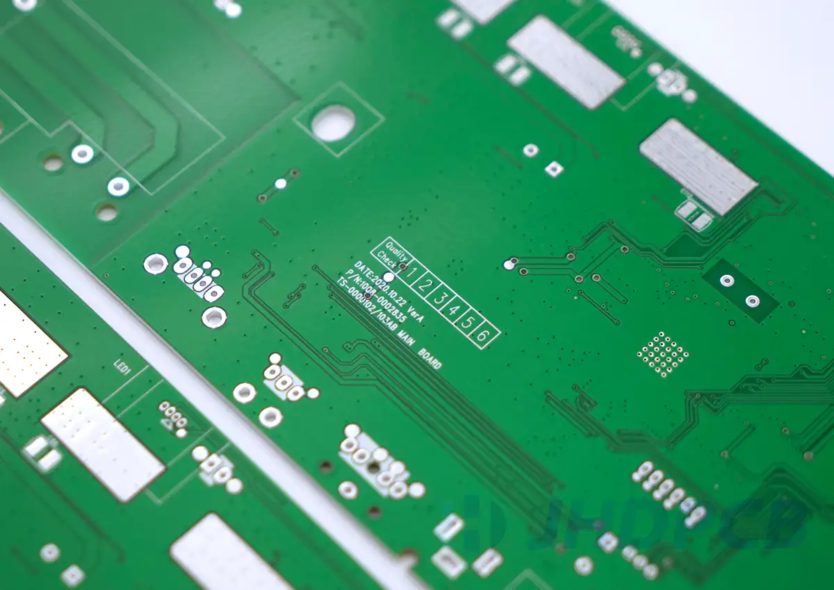
The Role of PCB Ground Plane:
-
Signal Return Path:
- The ground plane provides a low-impedance path for the return currents of signals, reducing electromagnetic interference (EMI) and maintaining signal integrity.
-
EMI Shielding:
- Acting as a shield, the ground plane helps contain electromagnetic radiation within the PCB, minimizing interference with other circuits and external sources.
-
Reference Plane:
- The ground plane serves as a stable reference point for signal voltages, aiding in noise reduction and ensuring accurate signal levels across the board.
-
Heat Dissipation:
- Ground planes can act as a heat sink, facilitating thermal management by dissipating heat generated by components mounted on the PCB.
-
Impedance Control:
- Ground planes assist in controlling impedance, particularly in high-speed digital circuits and high-frequency applications requiring precise signal integrity.
Design Guidelines for PCB Ground Plane:
-
Continuous Ground Plane:
- Ensure an uninterrupted ground plane across the PCB to minimize ground loops, reduce EMI, and provide a consistent reference potential for signals.
-
Split Planes:
- Use split ground planes only when necessary to isolate analog and digital circuits or manage different voltage domains, ensuring proper return paths and minimizing interference.
-
Via Placement:
- Place vias strategically to connect signal traces to the ground plane efficiently, reducing loop area and maintaining signal integrity.
-
Decoupling Capacitors:
- Position decoupling capacitors close to components and vias connecting to the ground plane to provide a low-impedance path for high-frequency noise.
-
Thermal Relief:
- Implement thermal relief on through-hole vias to connect to ground planes, balancing conduction and heat dissipation without compromising signal integrity.
-
Guard Rings:
- Use guard rings around sensitive components or high-speed signal traces to prevent interference by maintaining a low-impedance pathway to the ground plane.
-
Avoid Signal Crossovers:
- Minimize signal traces crossing split ground planes to prevent signal integrity issues and ensure clear return paths to the appropriate portion of the ground plane.
-
Bypassing Components:
- Bypass components (like resistors, inductors, or unused components) to the ground plane to reduce stray capacitance and improve performance by maintaining a stable reference potential.
-
Consideration for RF/Microwave PCBs:
- For RF and microwave PCB designs, ground plane partitioning and controlled impedance are critical to ensure signal performance and reduce signal loss.
By following these design guidelines and understanding the pivotal role of the ground plane, designers can optimize PCB layouts for improved signal integrity, EMI shielding, thermal management, and overall circuit performance.
