
Large steel buildings, cars, mountains, and even people can survive real atmospheric lightning. Humans can also create their own miniature lightnings (sparks) and survive. However, when these sparks reach the IC, they can cause major failures. In this tutorial , we will discuss ways to protect printed circuit boards(PCBs ) from ESD damage. We will demonstrate that analog parts with larger geometries are best suited for securing Field Programmable Gate Arrays (FPGAs ) with their smaller geometries. By taking these measures, the ICs in the FPGA maintain higher reliability and provide consistent quality performance.
Equipment, regardless of stature, is bound to be affected by lightning, steel buildings, cars, mountains and even people. In this application note, we will explain the mechanisms that protect ICs from ESD damage. Protecting ICs and circuit boards from ESD and EOS damage is a critical aspect of product reliability and performance.
Lightning can be fun and interesting, or dangerous and destructive. Maybe all of these things happen at the same time - it just depends on where you are, what you are doing and how tall you are. Thunderbolt is always bad for ICs.
A few years ago, we lived in a 10-story steel hotel building. Afternoon thunderstorms cut through a wide clearing. We felt comfortable and safe thanks to the steel frame of the building. Not plugged into our computer , so no worries. It was a spectacular show that lasted about 10 minutes as the storm passed.
Large steel buildings, cars, mountains, and even people can survive real atmospheric lightning. Humans can also create their own miniature lightnings (sparks) and survive. However, when these sparks reach the IC, they can cause serious failures. Nanoscale transistors need protection to survive even a human spark. In this tutorial, we will discuss ways to protect printed circuit boards (PCBs) from ESD damage. We will demonstrate that analog parts with larger geometries are best suited for securing field programmable gate arrays (FPGAs) with their smaller geometries. By taking these measures, the ICs in the FPGA maintain higher reliability and provide consistent quality performance.
from two angles
Sparks Where do artificial sparks come from? They are caused by triboelectric charging. It's a big word. This happens when two materials come into contact (aided by friction) and then separate. Some electrons will transfer to one of them. How many electrons move and to which surface depends on the composition of the material. This is a common phenomenon because almost all materials, insulators and conductors exhibit triboelectric properties. We are familiar with many common resources. Stroking a cat's fur, rubbing a balloon on a person's hair, and walking across a carpet can all exhibit the triboelectric effect.
No wonder it hurts when we walk over the rug and touch the doorknob! The general rule is that 5,000 V can jump about 1 cm (0.4 in) in 50% RH air. For someone five or six feet tall, it's the spark. It was painful, but we survived. Now, change your opinion. Could this spark cause damage several microinches high to transistors in integrated circuits (ICs) ? In this case, a one-centimeter spark is a huge, frightening display of lightning.
Now, let's talk about integrated circuits. Microprocessors have long been increasing the density of digital semiconductors.Manufacturing techniques have resulted in smaller and smaller transistors. In 1971, the Intel 4004 computer processing unit (CPU ) was introduced in 10 µm geometry . In the 1980s and 1990s, the process made parts smaller than bacteria. In 2012, ICs were 1,000 times less dense than 1971 technology, and the features on a chip were smaller than a virus. In 2012, one could buy a 28 nm-capable FPGA and a package of 6.8 billion transistors, and the future is expected to double the density in the next few years. Small transistors are tightly packed together and need to operate at low voltages (usually 1 V and below) to control the heat generated.
To see through 28 nm, note the zero: it is 2.8 billionths of a meter (0.000000028). Let the distance between San Francisco and New York City represent one meter (about 4000 kilometers or 2500 miles). Now 28 nautical miles (one of 36 million parts) is 0.11 meters or 4.4 inches. How much lightning does a device of this small geometry have to be damaged by? How to protect this necessary and useful FPGA?
The simple answer is to use an I/O interface device that bridges the digital and analog worlds. Analog mixed-signal ICs are relatively large in geometry ( 10 to 100 times larger than digital ICs) and have higher voltages (typically 20 V to 80 V or more), which make them more robust than tiny digital transistors . Although today's analog mixed-signal devices are generally ESD tolerant, they do benefit from discrete ESD devices.
Understanding Spark Corruption
Semiconductor manufacturers take electrical overload (EOS) and electrostatic discharge (ESD) very seriously. First, for obvious reasons, EOS and ESD can damage parts during manufacturing, package assembly, and testing. But more importantly, these negative forces will directly affect the quality and service life of the circuit in the customer's hands.
Initially, the electrically stressed part may appear to be functioning normally. It may even operate in a slightly degraded fashion and still pass the automatic test equipment (ATE) inspection, only to fail in the field later. EOS and ESD failures are preventable and undoubtedly critical quality control issues.
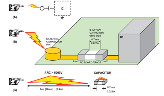
EOS and ESD damage is most likely to occur in manufacturing where ICs are made. Figure 1A shows a schematic diagram of the PCB. We might think that the IC is protected by a series capacitor . This is not the case. The second chance for damage is when the customer mounts the IC on the PCB to make the product. Looking closely at Figure 1B, we can see that the capacitor Since the spark just jumped 0.4" (1cm), the small gap around the capacitor is vulnerable to damage. The result may be that the IC pays for its life (Fig. 1C). Finally, EOS or ESD damage can occur when customers operate the product in their environment.
Of course, there are plenty of opportunities for huge losses. We can actually see the result of EOS and ESD damage inside the IC. For this, the epoxy material of the packaging must be removed . This is usually done with hot acid in a double glove isolation box. This process is very dangerous. Smoke is deadly. One breath can lead to a painful death. A drop of acid on a person's skin can at best result in amputation of a hand or arm, and at worst, death.
The photomicrograph of Figure 2A shows no apparent damage. Bond wires and pads marked REF are provided so we can orient and compare photos. Liquid crystal material is applied to the mold (pink), similar to the liquid crystals used in mood rings and children's forehead thermometers. With small changes in temperature, the color will also change. When the IC is energized, the area that draws excess current (marked here with a yellow box ) heats up and changes color.
Edit: Lisa Wang