
1. Detailed explanation of relevant design parameters:
1. line
Minimum line width: 6mil (0.153mm). That is to say, if the line width is less than 6mil, it will not be able to produce, (the minimum line width and line spacing of the inner layer of the multi-layer board is 8MIL)
if the design conditions permit, the larger the design, the better, the larger the line width, the better the factory production, and the higher the yield. It is very important that the general design routine is around 10mil, and the design must be considered.
Minimum line spacing: 6mil (0.153mm).. The minimum line spacing is line to line, and the distance from line to pad is not less than 6mil. From the production point of view, the bigger the better, the general routine is 10mil. Of course, under the condition of the design, the bigger the better. This point is very important. Must be considered.
Line to outline line spacing 0.508mm (20mil)
two. Via vias (commonly known as conductive holes)
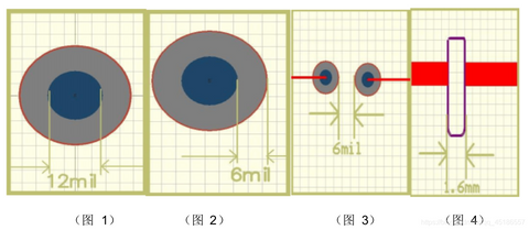
The minimum via hole (VIA) diameter should not be less than 0.3mm (12mil), the single side of the pad should not be less than 6mil (0.153mm), preferably greater than 8mil (0.2mm) must be considered
Via hole (VIA) hole to hole spacing (hole edge to hole edge) can not be less than: 6mil preferably greater than 8mil This point is very important, the design must be considered
Pad to outline spacing 0.508mm (20mil)
three. PAD pad (commonly known as plug-in hole (PTH))
The size of the plug-in hole depends on your components, but it must be larger than your component pins. It is recommended to be larger than at least 0.2mm, that is, 0.6 component pins. You must design it at least 0.8 to prevent machining tolerances. makes it difficult to insert,
Plug-in hole (PTH) pad outer ring should not be smaller than 0.2mm (8mil) on one side
Plug-in hole (PTH) Hole-to-hole spacing (hole edge to hole edge) can not be less than: 0.3mm, of course, the bigger the better (as shown in Figure 3) This point is very important and must be considered in the design
Pad to outline spacing 0.508mm (20mil)
Four. Solder mask
The plug-in hole opens the window, and the single side of the SMD window cannot be less than 0.1mm (4mil)
Fives. Character (the design of the character directly affects the production, whether the character is clear or not is very related to the character design)
The character width cannot be less than 0.153mm (6mil), and the character height cannot be less than 0.811mm (32mil). The relationship between the width and height ratio is preferably 5. That is to say, the character width is 0.2mm and the character height is 1mm, and so on.
Six: The minimum spacing of non-metallic slotted holes is not less than 1.6mm, otherwise it will greatly increase the difficulty of edge milling
Seven: Imposition
There is no gap in the imposition, and there is a gap in the imposition. The imposition gap of the gap imposition should not be less than 1.6 (the thickness of the plate is 1.6) mm, otherwise it will greatly increase the difficulty of milling. The gap of the imposition is about 0.5mm, and the craft edge cannot be less than 5mm
Two: Relevant matters needing attention:
One, the original document about the PADS design.
Copper is preserved (copper with Flood) to avoid short circuits.
In the double-panel file PADS, the hole attribute should select the through hole attribute (Through), and the blind buried hole attribute (Partial) cannot be selected, and the drilling file cannot be generated, which will lead to missing drilling.
Do not add slots in PADS design with components, because GERBER cannot be generated normally, in order to avoid leakage, please add
slots in DrillDrawing.
2. Documents about PROTEL99SE and DXP design
The solder mask of our company is based on the Solder mask layer. If the solder paste layer (Paste layer) needs to be made, and the multi-layer (Multilayer) solder mask window cannot generate GERBER, please move to the solder mask layer.
Do not lock the outline in Protel99SE, and GERBER cannot be generated normally.
Do not select the KEEPOUT option in the DXP file, it will screen the outline and other components, and cannot generate GERBER.
Please pay attention to the design of the front and back of these two documents. In principle, the top layer is the orthographic, and the bottom layer should be designed to be reversed. Our company superimposes the board from the top to the bottom. Special attention should be paid to single-chip boards, do not mirror randomly! If it's bad, it's the opposite
three. Other considerations
The shape (such as board frame, slot, V-CUT) must be placed on the KEEPOUT layer or the mechanical layer, and cannot be placed on other layers, such as the silk screen layer and the circuit layer. All grooves or holes that
need to be mechanically formed should be placed on the first floor as much as possible to avoid leakage grooves or holes.
If the shapes of the mechanical layer and the KEEPOUT layer are inconsistent, please make special instructions. In addition, the shape should be given a valid shape. If there is an inner groove,
the line segment of the outer shape of the board at the intersection with the inner groove needs to be deleted to avoid missing the inner groove. The grooves and holes designed in the mechanical layer and the KEEPOUT layer are generally made without copper holes (copper should be removed when making the film
). If it needs to be processed into metal holes, please make special remarks. If you want to make metallized slots, the safest way is to put together multiple pads. This approach must not go wrong.
When placing an order for the Gold Finger Board, please note whether it needs to be chamfered.
For GERBER files, please check whether there are few layers in the files. Generally, our company will make them directly according to the GERBER files.
With three software designs, please pay special attention to whether the button position needs to be exposed to copper.
Under normal circumstances, gerber uses the following naming methods:
Component surface line: gtl Component surface solder mask: gts
Component surface character: gto Welding surface line: gbl
Welding surface solder mask: gbs Welding surface character: gbo
Shape: gko Split hole diagram: gdd
drill hole: drll
PCB routing experience
In PCB design, wiring is an important step to complete product design. The following are only some wiring experience sharing in vulgar PCB design, and some are not suitable for high-speed PCB design.
In addition, the design process of the PCB board is a complex process, and I personally think that it needs continuous learning and recording, and continues to accumulate. This is an experience-building process.
The edges of the input end and the output end should avoid being adjacent and parallel to avoid reflection interference. If necessary, ground wire or power wire should be added for isolation; the wiring of two adjacent layers should be perpendicular to each other or intersect or even bend, and parasitic coupling is easy to occur in parallel.
Ground wire > power wire > signal wire, usually the signal wire width is: 8mil ~ 12mil; the power wire is 50mil ~ 100mil. The specific power line width can be queried for its load capacity. Generally speaking, pads, vias, etc. should be wider than lines.
The power traces should follow a tree-like structure, and the closer they are to the ends, the thinner they are.
Attention should be paid to isolation between high current signals, high voltage signals and small signals (the isolation distance is related to the withstand voltage to be endured. Usually, the distance between the board is 2mm at 2KV, and the ratio should be increased above this. For example, if you want to withstand a 3KV withstand voltage test, the distance between the high and low voltage lines should be more than 3.5mm. In many cases, in order to avoid creepage, a slot is also made between the high and low voltage on the printed circuit board.)
The corners of the wiring should be as large as 90 degrees as much as possible, avoid corners below 90 degrees, and use 90-degree corners as little as possible. Right-angle traces will change the line width of the transmission line, causing discontinuities in impedance. In fact, not only right-angle traces, but also sharp-angle traces may cause impedance changes. Especially for the design of high-speed boards, we must pay attention to this aspect. The influence of right-angle wiring on the signal is mainly reflected in three aspects: first, the corner can be equivalent to a capacitive load on the transmission line, slowing down the rise time; second, the impedance discontinuity will cause signal reflection; third, the right-angle tip produces EMI.
The distance between the legs of standard components is 100mil (2.54mm)
The copper on the edge of the board should be 20mil away from the edge of the board.
The traces should go as far as possible on the welding surface, especially the PCB with the through-hole process.
The grounding points of the same level of circuit should be as close as possible, and the power supply filter capacitor of this level of circuit should also be connected to the grounding point of this level.
10. As the heart of the single-chip microcomputer, the crystal oscillator must be as close to the chip as possible. In the minimum system of the single-chip microcomputer we designed, in addition to the crystal oscillator of the single-chip microcomputer, there is also a crystal oscillator for the usb-to-serial chip.
Use of shortcut keys
The use of shortcut keys can greatly improve the speed of drawing boards. Of course, you can also change the shortcut keys according to your needs. AD20 has a lot of shortcut keys, the following are just a few commonly used by me.
A method of modifying the line width before routing. After executing the trace command and pressing the start point, Track Width will be displayed in the lower right corner of the screen, which is the current line width. At this point, you can press the Tab key to modify the line width. This line width is maintained until the line width is modified in the next routing.
T+A+A reset first and then update (processing order, that page, starting index 1 + tick, reset all + update changelist).
Highlight: CTRL+click the mouse.
Q can change the unit mil-mm.
Copy pad: ctrl+c and then hold ctrl+v and drag to copy.
CTRL+M draws the ruler, SHIFT+C clears the ruler.
Board frame definition: Select a line, press TAB, all connected lines are selected, switch to the mechanical layer, shift + s to select the board frame and press DSD.
The silkscreen becomes smaller: select a silkscreen, right-click to find similar objects, and change the values of text height and Stroke Windth to recommend 10, 5moil. CTRL+A selects all, AP changes the identifier position.
Device move layer: Press L to move from the top layer to the bottom layer in the dragging state.
A+T: Top alignment. A+L: Left-aligned. A+R: Align right. A+B: Bottom aligned.
Spacebar: Flip and select an object (wire, via, etc.), and press the "Tab" key at the same time to change its properties (wire length, via size, etc.).
P+T wiring
T+E Teardrop
Ctrl + H Select the wiring of a certain network under PCB, it is easy to delete the wiring of the same network
Shift+S switches single-layer display and multi-layer display, Ctrl+shift+wheel switches layers
T+S schematic and PCB crossover selection. That is, select a component in the schematic diagram, and the component will be highlighted in the PCB diagram.
Summary of mistakes and problems
The page size should be unified with A4, if one page is not enough, there are several more pages, and the schematic style should be unified.
File naming. When a single schematic file is used, the schematic file can be named with the project name. When there are multiple files, add the prefix 00_, 01_, such as 00_Info, 01_Power, 02_MCU. The PCB file uses the project name and the version suffix, such as FB50_V1.0, 00_info , draw a table, the content is the function of each microcontroller pin, the internal resources used. For example,
PA9 serial communication UART1
PA0 LCD backlight control TIM2_CH1
PB3 clock IC IIC_SCL IIC2
Add a text document in the same directory of the project, name version record.txt. Used to record version updates
When sending pictures to others for review, in addition to the source files, export the schematics to PCB without adding PCB files.
Do not leave large blanks in the schematic diagram,
The network number of the schematic diagram, even if it is directly connected to the pins of the chip, should be drawn.
Pay attention to heat dissipation: For high-power circuits, those heating elements such as power tubes and transformers should be placed as far as possible in a distributed layout to facilitate heat dissipation and away from electrolytic capacitors to avoid aging of the electrolyte.
For the problem of copper laying, the test board should be all coated with copper, otherwise the reference plane is different, which may bring unexpected problems.
It is still the problem of copper laying. The PCB must have the shape structure of the mechanical layer and the KeepOut layer. The copper laying cannot reach the edge, otherwise it may cause a short circuit to the casing when installing the metal casing.
Do not block the traces or other components in the schematic diagram of the capacitor and resistor model. If you can't open it, open it in the wrong direction, or put a few more pages of the schematic diagram.
The power traces should follow a tree structure, and the closer to the end, the thinner
Decoupling capacitors, follow the small capacitors close to the chip pins, whether it is DCDC or power IC
The coordinate center point of the PCB file editing interface should be placed at the center point of the PCB board, or in the lower left corner, which is convenient for layout
The layout of the PCB depends on the appearance. The casing should be installed horizontally, and the PCB should also be designed horizontally. If there is a model of the casing, it should be put into the PCB for reference to prevent interference.
Compatibility design of multiple devices using the same PCB with no or very little cost increase
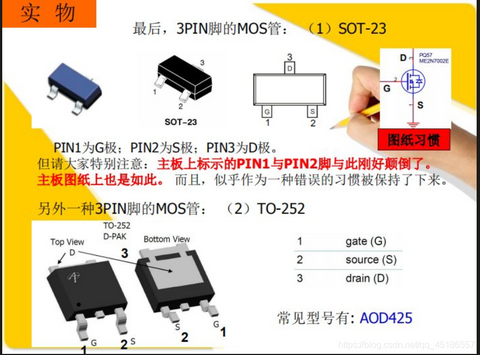
For the MOS tube with three PIN pins, the schematic diagram and real object of the PIN1 and PIN2 pins are generally reversed。
The ripple of the switching power supply is relatively large, and the decompression disorder after adding the load is very likely to be a problem with the PCB layout
For packages such as 0805 and 0603, the wiring must be uniform, otherwise, uneven heating may occur during soldering and a "tombstone" phenomenon may occur.
The crystal oscillator takes the differential line as close as possible to the microcontroller.
After opening the window, punch more holes to increase connectivity.
The convenience of production, debugging, and maintenance must be considered. For a PCB with a shell, the impact of the shell on its network port, USB port, etc. must be considered.
Obtain the schematic diagram and package of components from Jia Li Chuang:
Select the schematic diagram or package you need from the Jia Li Chuang mall or website, select use immediately。
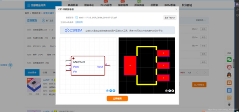
Export to the format required by AD, then download and save.
Open the file you downloaded with AD, save it as a schematic library or package library, and then import it into your own AD library.
The specific content will not be repeated, just Baidu.
The above article is based on the daily accumulation of many big brothers and myself. If there is any inappropriateness, you are welcome to criticize and correct.