
1. Antenna part design
1. The wiring from the Bluetooth IC to the antenna should be smooth or straight;
2. There should be no components, wiring and copper plating around the effective part of the antenna and its lower layer (ie, the back);
3. The antenna is required to be designed on the edge of the PCB board, facing the front panel as much as possible, and it is required to avoid iron structural parts around it;
4. Select the antenna type according to the size of the PCB board, select the inverted F antenna when the size is larger, and select the serpentine antenna when the board is small;
Second, the principle of component placement
The general order of component placement: first, place components that closely match the structure, such as power sockets, indicator lights, switches, connectors, interfaces, etc.; secondly, place special components, such as large components, heavy components , heating components, IC, etc.; finally, place small components; component layout should consider wiring, and try to choose a layout design that is conducive to wiring;
1. The crystal oscillator should be placed close to the IC;
2. The layout of the IC decoupling capacitors should be as close as possible to the power pins of the IC, and the circuit formed between them and the power supply and the ground should be the shortest;
3. Generally, the heating elements should be evenly distributed to facilitate the heat dissipation of the single board and the whole machine, and the temperature sensitive devices other than the temperature detection element should be kept away from the components with large heat generation;
3. Alignment principle
1. The high-speed signal traces should be as short as possible, and the key signal traces should be as short as possible;
2. Do not make too many vias for a trace, and do not exceed two vias;
3. The corners of the wiring should be as large as 90 degrees as much as possible, avoid corners below 90 degrees, and use 90-degree corners as little as possible;
4. When double-sided wiring, the wires on both sides should be perpendicular to each other, obliquely, or bent to avoid being parallel to each other to reduce parasitic coupling;
5. The audio input line should be of equal length, the two lines should be placed close to each other, and the audio line should be outsourced to the ground wire;
6. The power amplifier IC cannot be routed under the power amplifier IC, and more holes are made under the power amplifier IC to connect to GND;
7. There is no ground wire layer in the double-sided panel. The ground wire of the crystal oscillator capacitor should be connected to the GND pin closest to the crystal oscillator on the device using the shortest possible wire, and the via hole should be minimized;
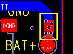
8. The power cable and the USB charging input should be thick (>=1mm), copper on both sides of the via hole, and then make a few more via holes in the copper layer, as shown in the yellow box below:
In general, the power and ground wires should be wired first to ensure the electrical performance of the circuit board. Within the scope of conditions, try to widen the width of the power supply and the ground wire. It is better that the ground wire is wider than the power supply wire. , the thinnest width can reach 0.05~0.07mm, and the power cord is generally 1.2~2.5mm.