
High-Density Interconnect (HDI) PCBs are designed to accommodate a higher number of components and connections in a smaller space. However, designing HDI PCBs can present challenges due to the increased complexity and density. Here are some tips to overcome HDI PCB design issues:
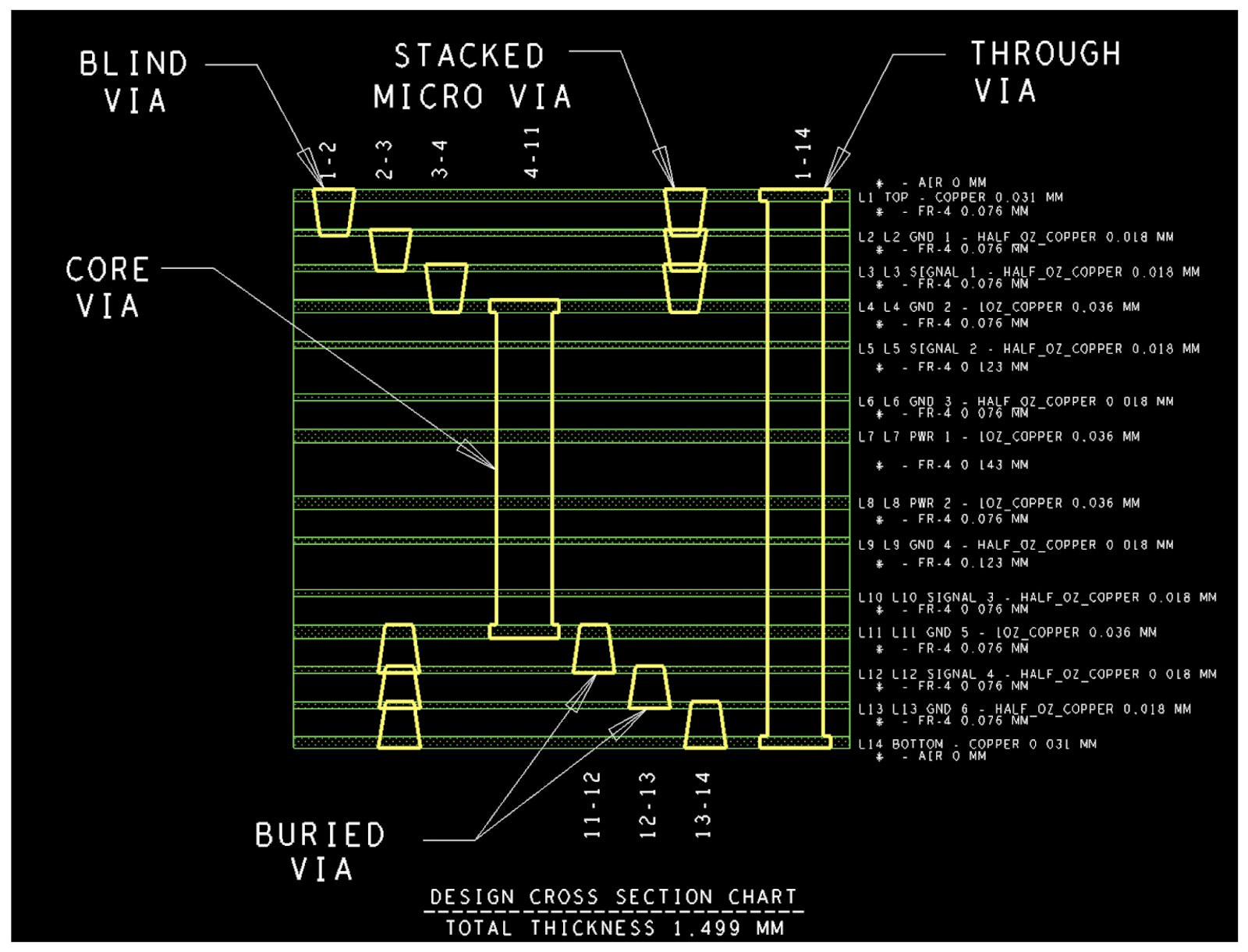
Figure 3: overlapping microvias (source: Cadence)
1. **Use Advanced CAD Tools:**
- Employ advanced Computer-Aided Design (CAD) tools specifically designed for HDI PCBs. These tools often have features like automatic routing, placement, and optimization algorithms that can simplify the design process.
2. **Layer Stackup Design:**
- Carefully design the layer stackup to meet the density and performance requirements. Consider using additional signal layers, microvia structures, and fine-pitch technology to accommodate the high-density components.
3. **Microvias and Via-in-Pad Technology:**
- Utilize microvias and via-in-pad technology to maximize routing density. Microvias allow for more compact designs and shorter signal paths. Via-in-pad technology can help reduce the number of layers needed.
4. **Aspect Ratio Consideration:**
- Be mindful of the aspect ratio of the vias, especially in high-density designs. High aspect ratios can lead to fabrication challenges. Ensure that the PCB manufacturer can handle the specified aspect ratios.
5. **Design for Manufacturability (DFM):**
- Collaborate closely with your PCB manufacturer during the design phase to address any manufacturability issues. Follow design for manufacturability guidelines to minimize the risk of errors during fabrication.
6. **Thermal Management:**
- High-density designs can generate more heat. Incorporate thermal management techniques such as strategically placing vias to create thermal paths, using copper fills for heat dissipation, and adding thermal vias.
7. **Signal Integrity and EMI Considerations:**
- Pay attention to signal integrity and electromagnetic interference (EMI) issues. High-density designs can be more susceptible to these concerns. Use proper impedance control, ground planes, and shielding techniques to mitigate signal integrity and EMI problems.
8. **Component Placement:**
- Optimize component placement for signal integrity and ease of routing. Group related components together and place critical components strategically. Consider using advanced placement algorithms provided by CAD tools.
9. **Routing Strategies:**
- Implement efficient routing strategies to minimize signal crosstalk and interference. Use differential pairs for critical signals, employ length matching, and carefully plan the routing paths to avoid signal degradation.
10. **Testing and Prototyping:**
- Prototype and test your HDI design to identify and address any issues early in the development process. Use simulation tools to verify the performance of high-speed signals and ensure they meet the required specifications.
11. **Documentation:**
- Create comprehensive documentation for your design. Clearly specify design constraints, rules, and guidelines for manufacturing. This will help both during the fabrication process and for future design iterations.
Remember, collaboration with your PCB manufacturer, careful planning, and the use of advanced tools are crucial for overcoming HDI PCB design challenges.