
The growing demand for more compact electronics requires multilayer PCBs and a 3D design perspective. This design perspective raises new questions about design strategies such as SMC (surface mount component) packaging and layer stacking. With the increasing complexity of the production of printed circuits consisting of multiple layers, the stacking of PCBs has greatly increased. The first prototype of the PCB was simple and used only as a connection base for electronic components. Given its simplicity, it is not necessary to stack multiple layers. Let's consider some rules to better design stacking systems to create highly specialized systems.
stack
Stacking involves assembling the copper and insulating layers that make up the PCB before designing the final configuration of the card. Achieving good stacking is not an easy task,
Multi-layer integration (see Figure 1) increases the power distribution capability of the card, reduces crosstalk, eliminates EMI and supports high-speed signals. While stacking levels allow multiple electronic circuits to be obtained on a single board through different layers of the PCB, the structure of the PCB stacking design has many other advantages:
1. Stacked PCB layers can help reduce the circuit's vulnerability to external noise and reduce radiation, impedance and crosstalk issues in high-speed systems.
2. Good PCB stacking can also facilitate low cost and efficient final production;
3. Proper stacking of PCB layers can improve the electromagnetic compatibility of your project.
For single-layer or double-layer PCBs, the thickness of the card is rarely considered. However, with the advent of multilayer PCBs, the stacking of materials started to become more and more important, and ultimately cost was the factor that affected the entire project. The simplest stack can include a four-layer PCB. The most complex requires professional sequential layering. The more layers, the more freedom the designer has to break the circuit, and the less likely an "impossible" solution will fall. The PCB stack-up operation involves stacking the copper and insulating layers that make up the circuit. The stack of choice can play a role in card performance in a number of ways.
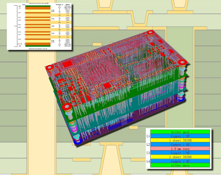
For example, proper layering can reduce the impedance of the card and limit radiation and crosstalk. It also has a significant impact on the EMC (Electromagnetic Compatibility) performance of the product. On the other hand, a misunderstanding of stacking can greatly increase radiation and noise in a circuit. There are four important factors to consider when stacking cards:
1. Number of layers;
2. The number and type of planes used (power and ground planes);
3. Classification and order of levels;
4. Spacing between levels.
Usually, these factors are hardly considered except those related to the number of layers. To determine the number of layers, the following elements will need to be considered:
1. The number of signals that must be sent and their cost;
2. Operating frequency;
3. Whether the product must meet the emission requirements of Class A or B;
4. Whether the PCB is intended to be part of the shield;
5. Whether the design team has expertise in EMC standards and regulations.
All factors are important and essential and must be treated equally. Multistory aircraft using mass and power plans can significantly reduce radiated emissions. A rule of thumb that is often used is that, all other factors being equal, a four-layer card produces 15 dB less radiation than a two-layer card.
Rules and standards for good stacking
Hundreds of rules and standards are necessary to achieve good stacking. Take a look at what's there:
1. High-capacity planar cards are preferred as they allow signaling in either miniature tape or balanced tape line configurations. They can also significantly reduce mass impedance, thereby reducing ground noise.
2. High-speed signals must be "routed" on the intermediate layer between the different levels. In this way, the ground plane can act as a shield and contain radiation from high-speed rails.
3. Even in adjacent planes, the signal layers should be very close to each other;
4. The signal layer must always be adjacent to the plane;
5. Having multiple ground planes is very advantageous because they reduce the ground impedance of the card and reduce radiation through current;
To achieve all of these goals, at least eight layers must be running. more importantly:
1. From a mechanical point of view, it is recommended to build a cross section to avoid deformation;
2. The configuration should be symmetrical. For example, on an eight-layer PCB, if level 2 is a plane, then level 7 must also be a plane; if level 2 is a plane, then level 7 must also be a plane.
3. If the signal level is close to the plane level (ground or power), the return current can flow on the adjacent plane, which minimizes the inductance of the return trace;
4. To further improve noise and EMI (electromagnetic interference) performance, the isolation between the signal layer and its adjacent planes can be even better.
5. An important consideration to consider is the thickness of each signal layer. There are standard thicknesses as well as the characteristics of different types of printed circuit materials. When choosing a material, it is recommended to consider its electrical, mechanical and thermal properties;
6. Use great software to help you design your stack. All of this is necessary to select a suitable material from the library and perform impedance calculations based on the material and its dimensions.
PCB needs careful design
Due to the high operating speeds of today's circuits, careful PCB design is necessary, which becomes an art in all respects. A poorly designed PCB can degrade the electrical performance of signal transmission, power distribution, productivity, and long-term reliability of the finished product.