
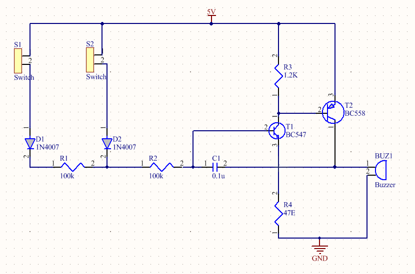
The schematic is a drawing that defines the logical connections between components on a circuit board whether it is a rigid PCB or a flex board. It basically shows you how the components are electrically connected. A schematic contains a netlist which is a simple data structure that lists every connection in the design, as specified by the drawing. The below image shows an example of a schematic diagram.
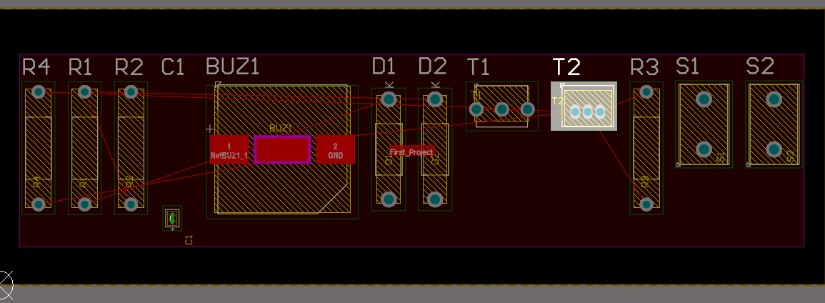
In contrast, the PCB layout shows the exact physical locations of every component on the PCB and shows the physical wires (traces) that connect them together. An example of a PCB layout is shown below.
RULES TO DRAW A SCHEMATIC
To achieve successful schematic design, follow the below rules:
- Electrical connections between the components are represented by lines. Lines that intersect with each other are not connected unless there is a node present at the point of intersection.
- It is always a good practice to have only 3 lines connected to a node.
- In complex circuits, it is recommended to assign names to nets. The nets with the same name are assumed to be connected.
- The pin numbers, polarity, values, and net names should be written horizontally.
- Place the inputs on the left and outputs on right.
- Design schematic sections in functional blocks.
- Always place pin numbers on the outside of the symbol graphic.
- Sheet connection symbols should always be placed on the extreme left edge or extreme right edge of the page.
- Place the title block on the lower right corner of the first sheet. The title block should display the following information:
- Title
- Part number
- Revision (if any)
- It is a good practice to have a page showing the block diagram of the circuit and also a history page that lists the changes in the schematic over a period of time.