
A printed circuit board (PCB) is the heart of electronic products. They provide the conductive pathway that allows all electronic components to function and connect. Multiple layers of PCBs are used to connect complex electronics.
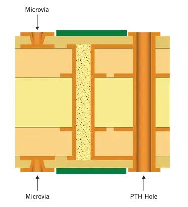
When copper is plated on the holes, holes are made through the PCB to route electrical connections between layers. These holes are known as vias (plated through-holes). The hole can be classified as a microvia, depending on its diameter.
What is a Microvia?
According to the Institute of Printed Circuit Boards, a microvia is any hole drilled in a PCB with a 1:1 aspect ratio and not exceeding 0.010 inches. The IPC used to consider microvias according to their size if they were smaller than 0.006 inches. With the advancement of technology, lasers can drill these small holes more often.
The IPC adopted the microvia definition of the 1:1 aspect ratio to prevent meanings from changing. Microvias, also known as uVias or microwires, can be used to connect layers within a PCB. They are usually limited to connecting two layers at a time.
The Different Types Of Microvias
PCB designers have many options for drilling microvias. Each microvia is the same in size. Their placement is the main difference.
- Blind Microvias- Drilled to allow connections between the surface and an inner layer. These holes are not as deep as a through-hole but only reach one side of the PCB.
- Buried microvias are holes in the inner layer of the PCB which do not reach the circuit board's surface.
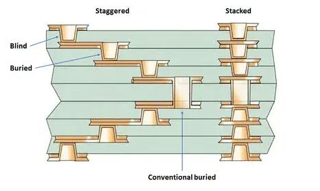
- Stacked microvia - several blind or buried microvia are stacked on top of each other to allow for the inner layers to be connected.
- Staggered microvias are layers of multiple buried microvia. These microvia do not stack on top of one another. They are instead placed in an offset fashion.
- Via In-Pad Microvias is a method of placing microvia holes directly ontothe copper solder pad. This allows PCBs to become miniaturized.
Advantages Of Microvias In PCB Design
Microvias can be used for circuit board designs by PCB designers. Microvias provide thermo-mechanical reliability for the functions and performance. The ability to make via-in-pad microvias allows the board to be miniaturized. Because microvias are smaller than standard vias or plated through holes, they save space on circuit boards. You don't need to have bigger boards to accommodate all the components.
Microvias can be used to minimize defects in PCB designs. Lasers are used for drilling the holes. Because the trace lengths of microvias are shorter, there are fewer fabrication problems. Microvias have significant effects on signal integrity when creating an HDI circuit board. Higher radiation levels are created by using larger vias for high-speed circuits. Microvias can enhance RF capabilities and EMC characteristics. Microvias are more reliable than other types of vias and through holes.