
Use block diagrams and title block
The block diagram in electronics design is viewed as the best reference material which shows the overview and the architecture of your schematic and helps the reader to quickly understand and introduce the circuit function by summarizing the systems and sub-systems of the design. Using a bloc diagram of DC regulated power supply which is represented in Figure 1 to introduce your hardware design to anyone who looks at and examines your circuit is the successful method that most designers neglect it.

Figure 1: Block diagram of DC regulated power supply
Another important rule is to give a name to your schematic and to add your name on the circuit at the Title Block which makes the schematic looks more professional and proficient. Figure 2 represents BCD to 7 segment schematic which includes the necessary and required detail and notes for someone to implement this circuit in the breadboard or build a Printed Circuit Board (PCB) layout.
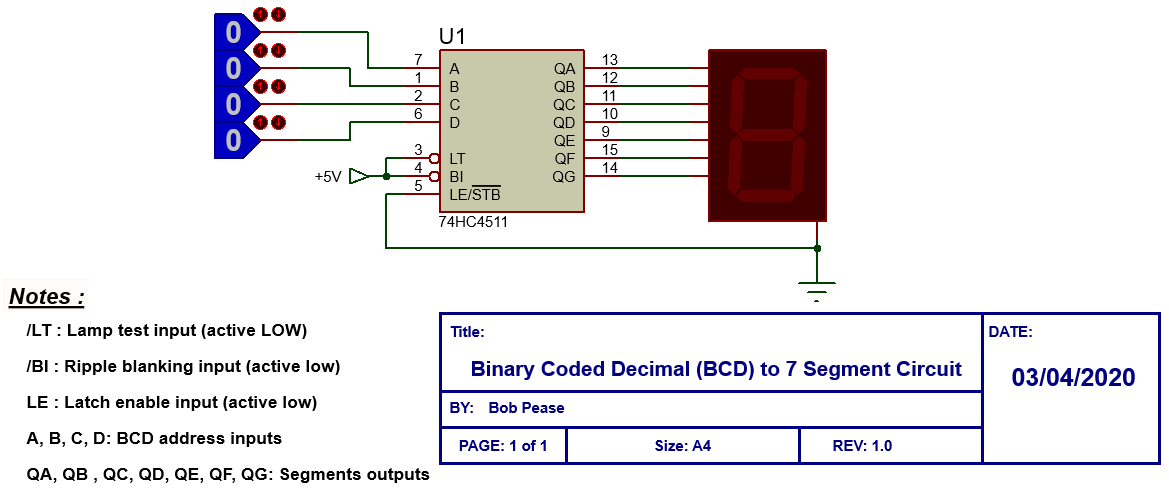
Figure 2: BCD to 7 segments schematic design
In the other hand, it is preferably to design your schematic for a regular size paper because almost readers have only access to standard page-size printers like A4 which is the most commonly used paper size. If your design needs more space, you can split your schematic into multiple design sheets in order to increase readability.
Parts and I/O signals placements
Your schematic should be drawn so that electrical signals start flowing from the left to the right. Figure 3 shows an amplifier circuit that the inputs are placed on the left and the outputs are placed in the right side. Conventionally, the power line should be at the top and the ground level at the bottom of the schematic in order to increase the readability.
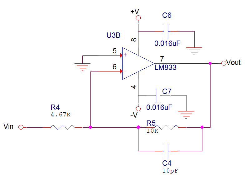
Figure 3: Operational amplifier circuit
The schematic design is viewed as an artistic process because each designer should give proper love and care during the component placement by grouping the similar components in the single and same direction mainly the polarized components in a single row or column as depicted in Figure 4 to reduce connection paths and to give for your other components such as Integrated Circuits (ICs) a room to breathe when passing to the PCB layout design.
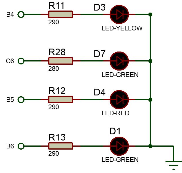
Figure 4: Grouping similar resistors and LEDs in a single column
All good ECAD offers the possibility to edit the grids in the schematic editor to enable easier components and pins placement. Generally, it is highly recommended to use 100 mils/2.54 mm grids for normal design and 50 mils/1.27 mm grids for dense schematics which permit to place any object in the gridline including its pins to avoid the disconnection of the parts.
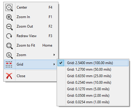
Figure 5: Grid size setting uding the free KiCAD tool
Clarify your connections
It is important to show and distinguish which nets are connected and which are crossed over. To overcome this issue, you have to use the dot convention to clarify your connections. The preferred methods are shown in Figure 6 to connect or to cross nets even the dot disappears due to photocopying problem.
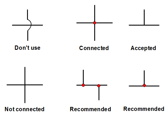
Figure 6: Rules for crossing or connecting nets
When connecting a symbol pin, it is recommended to advance at least one grid point straight out before a direction change as shown in Figure 7. This tip ensures that all nets in your schematic will appear in the netlist while producing the PCB layout.
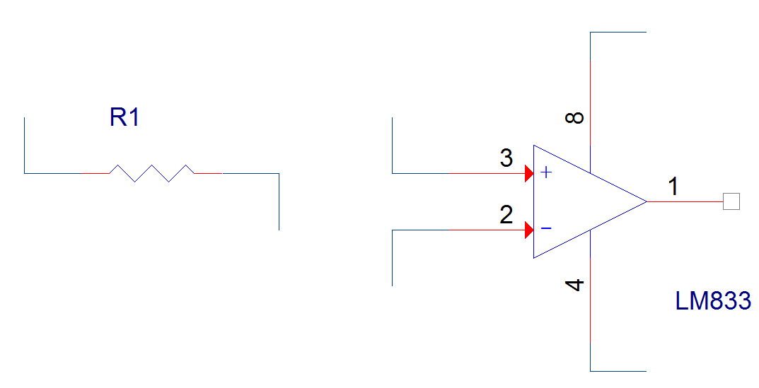
Figure 7: Connecting nets to pins
You can use busses to group signals when it is possible and necessary to increase readability and to make your schematic more concise. For example, it is useful to use a bus to connect 10-channel ADC (Analogue to Digital Converter) to your analogue sensors as. This feature is supported in all good ECAD tools have the capability of grouping signals.
You can also employ a global connector or symbol to create a connection between different wires to common signals for hidden power pins such as ground and power as represented in Figure 8 via hierarchy (sub-circuits, hierarchical blocks and multiple-pages) and to make the schematic more concise without clutter. Referring to Figure 9, +V and –V signals and VIN and VOUT are global connectors which are used to hide the bypass capacitors from the signal path in order to minimize clutter.
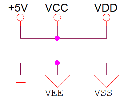
Figure 8: Method of connecting hidden power pins using global connectors
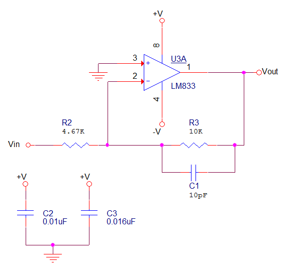
Figure 9: Employing global connectors in a schematic
Use nets labels and concise reference designators
Your schematic should have all the nets labelled mainly for the important signals. This task will help you during debugging or when running simulations and even in PCB layout design. Even labeling the nets are optional and not necessary but it will save a lot of time mainly during PCB layout design. In Figure 10, both Reset and LED signals are nets labels. Another important key of labeling nets is to increase the readability by connecting far terminals even they are not connected physically through a wire as depicted in Figure 11.
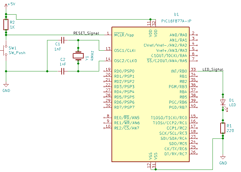
Figure 10 : Using Nets name for important signals
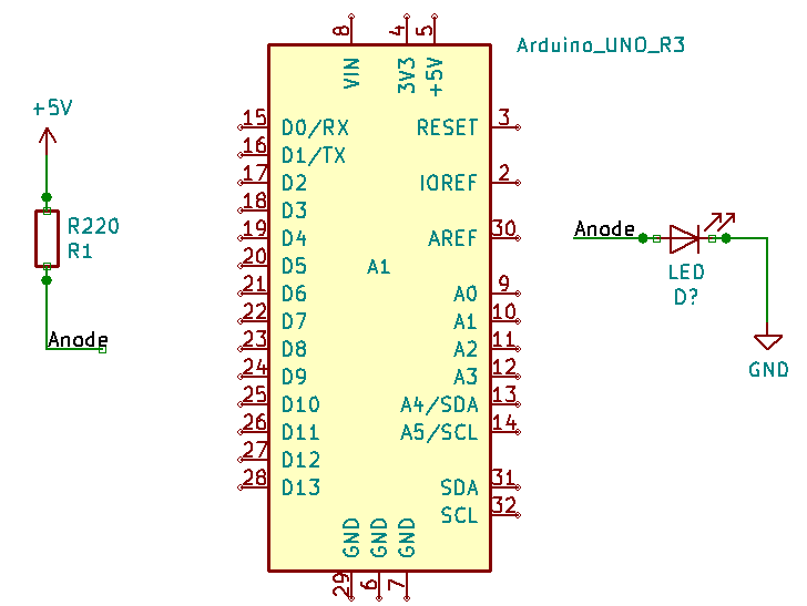
Figure 11: Using Nets labels for far connection
Another very important key that you have to take care about is Reference Designators and the proper values which are the number / letter combinations to show and identify the component type according to Table 1 in your design. These references are generally printed on a PCB as labels which allow finding easily components location. In your schematic, references should be found close to the component according to a pattern that you choose for your entire design above or below horizontal components and left or right of vertical components as represented in Figure 12.
Table 1: Common reference designators
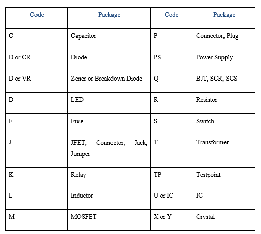
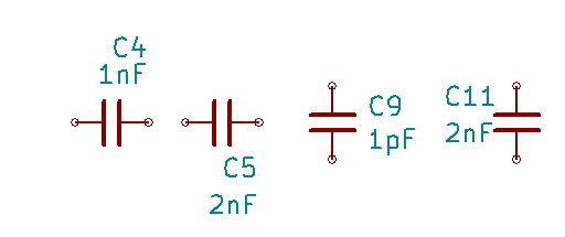
Figure 12: Positioning reference designators
When you want to write down over your diagram for notes or other purposes, make sure to be consistent, short and concise with your naming task. Try to use blank space between names to minimize the clutter of mixing the schematic with your writing which may get the readers confused.
Filter your Input and Output Signals by using coupling and decoupling capacitors
We will talk about capacitors which are known by their filtering feature which is used by schematic designers.
Generally, power supplies are not stable and deliver an output voltage that will be fluctuating which may damage the circuit mainly when powering microcontroller boards. For this reason, you should add a capacitor in parallel and near to the power source while designing your circuit to provide pure DC supply. In this case, this capacitor is called DECOUPLING CAPACITOR. This decoupling capacitor starts charging from the source and when the Vcc voltage level is attained, the current will not flow via the capacitor. The decoupling capacitor will maintain and hold this charge until there will be a drop in voltage level from the source.
Another important key that you have to keep it in your mind when dealing with the amplifier circuit is to use coupling capacitors. These coupling capacitors permit to smooth and block both the low-frequency noise and DC element in the output signal of an amplifier circuit.
Therefore, the bypass capacitor is used to eliminate inter and intra noise from the system by bypassing it to the ground mainly in amplifier and loudspeaker circuits to get clear audio. The value of this capacitor is selected by the famous formula C = 1/ (2πfXC) and by assuming that the capacitor reactance (Xc) should be 1/10th or less than the resistance in parallel.
To sum up, keep in your mind that decoupling capacitors are useful for incoming signals to decoupling AC from DC signals where their values should be between 1 µF to 100 µF at low-frequency noise and between 0.01 µF to 0.1 µF at high-frequency noise. However, coupling capacitors are used for outcoming signals. The bypass capacitors are useful for removing AC noise from a DC signal to get a pure and cleaner DC signal. The three different types of mentioned capacitors for filtering purpose are grouped in Figure 13.
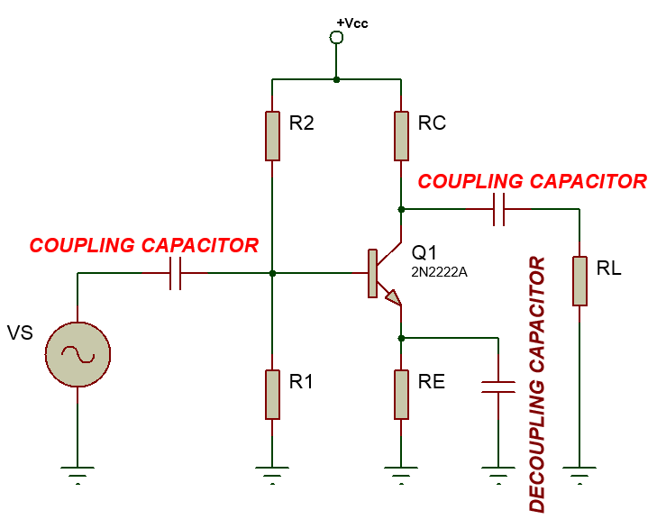
Figure 13: Using capacitors for filtering
Use pull up & pull down resistors
This golden rule should be kept in your mind automatically when dealing with microcontrollers and digital IC circuits to avoid and overcome the floating state or third state as it is known in digital electronics literature.
As you know that each digital IC works with logic levels that have a direct relation with the input voltage. For example, the input voltage between +5 volts to +2.8 volts in a digital IC will be interpreted as high state or Logic 1 and 0 volts to +0.8 volts will be interpreted as low state or Logic 0. Otherwise, this input voltage between +0.9 volts to +2.7 volts will be an indeterminate state or floating state and in this case, the logic state will be either a low (0) or a high (1).
You can bypass the above-mentioned scenario by using resistors component to force the desired voltage in the input chip pins. In this case, you should use Pull up resistors (generally 4.7 kΩ) which are represented in Figure 14 to apply and force the voltage near to Vcc (+5 volts or 3.3 volts) and Pull-down resistors (generally 10 kΩ) which are shown in Figure 15 to force the voltage near to the ground voltage level (0 volts). The unknown state in the chip or Microcontroller inputs can be easily avoided and now you are sure that your digital ICs will behave correctly.
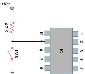
Figure 14: Using Pull up resistor in the IC input
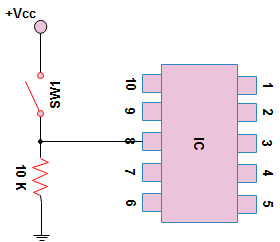
Figure 15: Using Pull down resistor in the IC input
Use microcontrollers (MCUs)
This tip will save you much time and reduce your schematic size by eliminating a lot of components to do a simple analogue to digital conversion for example which you will find it easily in one single microcontroller (MCU) chip with other pretty functions but you must program your MCU and read its datasheet.
Modern MCUs from different brands (ATMEL, Microchip, STMicroelectronics…) offer advanced features with low-cost prices to achieve many tasks such as Serial/I2C/SPI communication, A/D Conversion, Timers, and much more all grouped in small packages which take less space and increase both the efficiency and the performance of your design.
Use PWM signals to save power consumption
Building a circuit that saves energy is very important mainly when your final product cannot be charged or you cannot replace its battery cells because it is deployed in the forest for example. For that reason, you should always think about using pulse width modulation (PWM) scheme by using NE555 or a dedicated MCU which can increase the energy efficiency of your application. This technique can be employed to save energy on simple LED or motor circuits.
To clarify this tip, we take for example a 50Hz PWM signal with 75% duty cycle. With these parameters, the ON pulse stays for 75% where the current flows and the OFF pulse (no current flows during this time) stays 25% for the whole time period. During the off-time, LEDs or Motors react slowly to this current transition which will give an impression that they are still staying ON. Figure 16 shows the commonly used duty cycles that you can employ according to your application to save power.
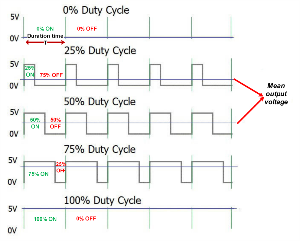
Figure 16: PWM technique to save power consumption
Choose the right standard for component symbols
Before you start designing your schematic, think about which components symbols that you want to use during your drawing. Even symbols are employed internationally but they differ in some places in the world mainly in the U.S. For example, the resistor symbol employed by many designers in the U.S. is different than in the European side as represented in Figure 17.
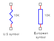
Figure 17: Commonly used resistor symbols
The Institute of Electrical and Electronics Engineers (IEEE) has developed many standards for commonly used components symbols to designers such as IEEE Standard 91 graphic symbols of logic functions, IEEE Standard 315 which includes graphic symbols and designation for both Electrical and Electronics Diagrams and IEEE Standard 991 for Logic Circuit Diagrams.
Another point that you should take care about is the capacitors symbols to avoid catastrophic accident including fire, smoke and explosion during implementation when dealing with polarized capacitors. For that reason, it is preferable to use symbols shown in Figure 18 for both polarized and non-polarized capacitors. This polarized capacitor symbol with the small “+” sign is very useful even this sign vanishes due to photocopying issue, you and readers will recognize this component quickly.
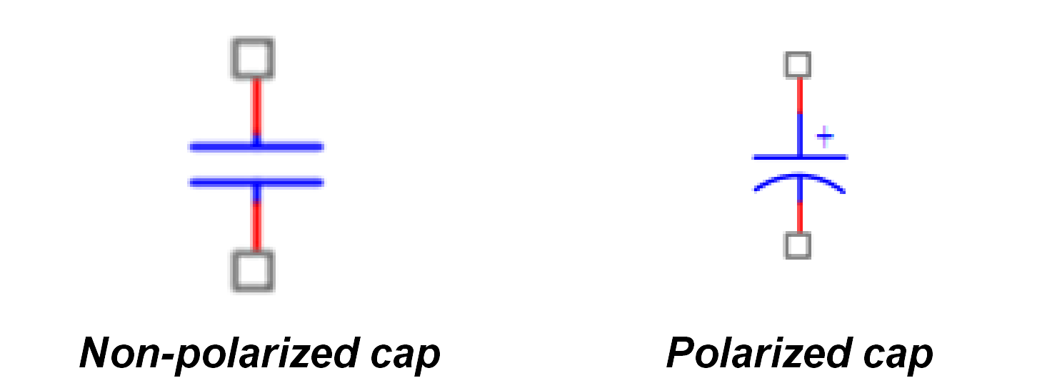
Figure 18: Preferred symbols for capacitor
Choose the right CAD tool
You can hand draw basic schematic designs easily even you aren’t an expert designer like Bob Pease. However, it is very beneficial to build your complex designs which may use many parts and integrated circuits using suitable Electronic Computer-aided design (ECAD) software also known as Electronic design automation (EDA). The ECAD software generally is selected by your company or your client and mentioned at the job description or in the ITB (invitation to bid). In the other hand, it is highly recommended to use a professional CAD from well-known developers that it is able to produce schematic, and PCB layout designs with 3D views, bill of materials (BOM), artwork, Gerber files for the final product production.