
Do you want to build a high-frequency PCB but don’t know what type to design? Then, you can try Teflon PCB.
Teflon PCBs are high-frequency boards with powerful features that make them suitable for various applications. But they require a lot of focus when handling them because they are a bit tricky to use.
But don’t worry. This article will introduce you to Teflon PCB and how you can build a high-speed Teflon PCB prototype.
What is a Teflon PCB?
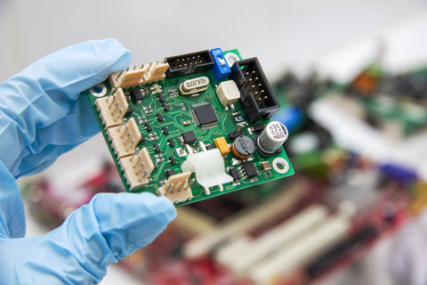
Man Holding PCB
A Teflon PCB is a high-speed board that utilizes PTFE (Polytetrafluoroethylene) as its base material. It’s capable of transmitting high-frequency signals of 5GHz and above, making it great for constructing PCBs with improved connections and capacities.
Teflon is not 100% PTFE. It’s a patent of PTFE, which Dupont named in 1941. Pure PTFE has a lubricating nature that makes bonding to copper layers difficult. Hence, most manufacturers reinforce PTFE with glass, woven, or ceramic to make the Teflon PCB substrate.
Plus, Teflon is one of the most popular materials manufacturers prefer using to fabricate high-frequency PCBs.
Properties of Teflon PCB
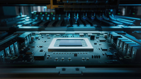
High-speed PCB
As we mentioned earlier, Teflon is pretty popular among manufacturers for PCB fabrication because of its excellent properties. These properties include:
Low Thermal Expansion
Teflon has high heat resistance, making it great for cookware. Because of this property, it’s also suitable for high-speed electronic devices that generate significant amounts of heat when operating. Plus, its Tg can be anywhere between 160 and 280˚C. Sometimes, it can have a Tg higher than 280˚C.
Additionally, Teflon boasts excellent thermal stability that enables it to retain its form and properties in extreme temperatures. Plus, it’s also fire resistant.
Fire Resistance
Low Dissipation Factor
Teflon is pretty resistant to current leaks because of this property. It’s one of the reasons why the material is suitable for microwave and high-frequency PCBs. Plus, its low dissipation factor also grants it incredible weather resistance.
High Chemical Resistance
Chemical Resistance
Teflon PCBs can resist chemical effects. For this reason, it has excellent corrosion and erosion resistance. Things like grease and moisture also won’t affect a Teflon PCB’s performance.
Increased Dielectric Properties
Teflon boasts low dielectric loss, allowing it to maintain a dielectric constant over high-frequency applications.
Low Friction Probability
Teflon has a smooth and non-stick surface, which significantly reduces the chances of friction damage.
Excellent Durability
PTFE PCBs offer increased durability, making them capable of maintaining excellent performance under extreme conditions and even withstanding damages from oxidation. Plus, they also boast incredible mechanical durability.
Teflon PCB Manufacturing
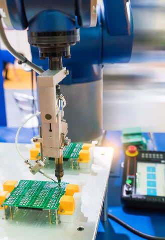
PCB Manufacturing
Here are some tips to help with the Teflon PCB manufacturing process.
How to Prepare the PCB Surface
What you need is sodium etching. It’s a process that will increase the Teflon material’s bondability. Then, all you have to do is soak the Teflon material in a sodium solution.
The solution shouldn’t be 100% sodium, but it should be the dominant element. After soaking, you can rinse with an H20 solution and some alcohol.
Alternatively, you can use plasma arc gratification. It’s a process that prepares your PCB’s surface for metallization, marking, and layer shaping.
Applying Solder Masks
A solder mask is an important material you must apply after etching. Plus, you’ll get better results if you do it in less than 12 hours after etching. Also, it’s best to bake the Teflon in an oven to remove any leftover moisture before applying the solder mask.
Copper Cladding
Copper Layer
You can’t do without copper cladding when it comes to PCB fabrication. It’s a universal phase that prepares the copper surface, drills the Teflon material, and plates the through-holes. Also, it’s best to use copper with incredible tensile strength so you won’t have lift pads and barrel cracks.
Laminating your Teflon PCB
If you’re not using bonding films or prepregs, you can laminate your Teflon PCB at 370°C and 450-500 pounds PSI pressure.
Using bonding films and prepregs with low melting points would help reduce the lamination temperature to 120°C or 215°C.
Moreover, some hybrid Teflon PCBs require a different lamination process. These hybrids combine Teflon and FR4 and need oxide pretreatment before laminating.
Drilling
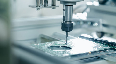
PCB Drilling
You’d need some specific equipment to drill on a Teflon PCB. The kind of drill you need for precise and clean holes is one with a high chip load. It will ensure there are no fibers left and prevent Teflon tailing.
Storing your Teflon Laminates
Teflon can create durable PCBs, but the laminates alone are soft and easy to damage. So, it’s crucial to handle them with care always. Also, avoid stacking them in ways that could potentially cause damage.
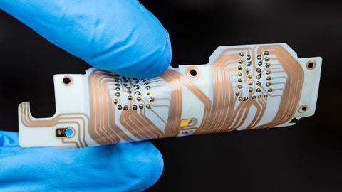
Types of Layers in a PTFE PCB
PCB Layers
A PTFE PCB can have two types of layers, including external and internal layers.
External Layers
These are the outer copper layers where you can attach your components. In addition, it includes a copper foil that you can electroplate with copper.
Electroplating helps to increase thickness and includes more copper in the thru-hole barrels. Plus, you can customize the final copper thickness to fit the applications of your Teflon PCB.
Internal Layers
The several copper laminates between the top and bottom layers constitute the internal layer.
Sometimes, you can use copper pour to create a power or ground plane inner layer. It can help the layer-to-layer bonding process and reduce the amount of etchant used when manufacturing.
Also, the copper thickness and weight depend on your PCB’s specifications. Similarly, the internal copper weight determines the minimum space and width you can fabricate.
Steps in the Production of a Teflon PCB Prototype
Here are some steps you can follow to help build a Teflon PCB prototype:
Step One: Make your Designs
You can make the designs for your Teflon PCB prototype with a stencil and PCB design software. Here, you must pay attention to your prototype’s general layout because you’ll use it for the final designs.
Step Two: Choose your Base Material
You don’t have to use PTFE when building your prototype—save it for the final designs. Instead, you can use plastic as a substitute material for PCB prototyping.
Step Three: Test your Design
There are two ways you can test your prototype. First, you can use a simulation or construct an initial prototype board. Design testing is crucial because it helps verify components and ensure they are in the correct position.
Step Four: Time to Troubleshoot
If you find any errors after your design tests, you can troubleshoot to fix them within your board’s design. You can find faults, including misplaced/faulty components or design bugs.
Step Five: Construct your Prototype and Test Its Functionality
After building your prototype, you’ll need to test its functionality. It’s the final step to ensuring your board is error and bug-free. When you’re satisfied, you can send your designs for manufacturing.
What are the Methods of Teflon Panelization?
There are two panelization methods you can use for Teflon PCBs, which include V-groove and tab-route. Let’s take a closer look at these methods:
V-Groove Panelization
For this method, you’ll need a triangular saw to cut through one-third of both panel sides. It’ll leave a thin section of Teflon holding two separate PCBs together. Plus, you can use simple tools to separate them when necessary.
V-groove only works for PCBs with straight lines separating them. And the cuts must be from one board edge to the other.
Tab-Route Panelization
Tap-route is a more flexble method for PCBs that don’t have straight and simple lines separating them. It also works for boards that include multiple designs.
For this method, you’ll use a router to cut through the Teflon between boards, leaving small tabs to keep them together during assembly. You can use depanelization tools to break the tabs or do it manually.
Perforated Tabs
Here, you’ll perforate tiny holes called mouse bites into your tabs. These holes make it easy to depanelize individual PCBs.
However, it’s crucial to sand after perforating to remove leftover materials from your PCB’s edges.
What are the Different Types of Layers in Teflon PCB Inner Layer?
Here are the different types of inner layers we have on a Teflon PCB:
Mechanical Layer
Your design will determine the number of mechanical layers your Teflon board will need. But, it needs at least one of these layers to fit the PCB’s physical dimensions.
Solder Mask Layer
It’s a layer of green protective film that prevents damage and contamination.
Keep Out Layer
Keep out layers state the working boundaries of Teflon PCBs.
Routing Layer
Routing layers are responsible for connecting the components of Teflon PCBs.
Solder Paste Layer
You’ll need solder paste layers on areas where you’re mounting components. It helps improve solder bonding and improves solder flow.
Power and Ground Planes
These copper layers link the power and ground planes to an onboard voltage terminal.
Split Planes
With this layer, you can separate the ground and power planes while connecting them to different voltage points.
Silkscreen Layer
The silkscreen layer is only for easy identification.
Advantages of Teflon PCBs
Here are some benefits you can enjoy from using Teflon fabricating material:
Impressive Dielectric Strength
Teflon PCBs have high dielectric strength, making them non-conductive. Hence, they are excellent insulators that can prevent electrical breakdowns.
Mechanically Rigid
Teflon PCBs can maintain their mechanical stability even under applications that require high mechanical stress.
Immense Durability
PTFE can withstand many things, making it one of the most durable materials available. It can resist oxidation, embrittlement, ultraviolet rays, and discoloration.
Its durability also makes it cost-effective as it can last for extended periods.
Applications of Teflon PCBs
You can use Teflon PCBs to produce the following devices:
- WiFi antennas
- Power amplifiers
- Wireless base stations
- Automotive cruise controls
- Thermal solutions
- Handheld cellular devices
- Telematics and infotainment devices
Costs of Teflon PCBs
There is no fixed cost for Teflon PCBs. Instead, several factors determine how much a manufacturer will charge. These factors include panel size, inspection charges, surface finish, size and number of drills, layers, and type and size of raw materials.
Rounding Up
High-tech PCB
Teflon PCBs are excellent boards for high-frequency applications. They can handle the heat generated from these applications and resist damage from chemicals, oxidation, and friction.