
THE PURPOSE OF PCB LAYER STACKUPS
A PCB stackup refers to the arrangement of copper and insulating layers that make up a PCB. These layers are arranged in a way to get multiple printed circuit boards on the same device. At their most basic, multilayer PCBs consist of at least three conductive layers. The bottom layer is synthesized with the insulation board, and each circuit board layer is connected to the next.
While PCB layering creates a more complex and space-saving board, PCB stackups also offer the following advantages:
- Maximize functionality: Multilayer PCBs can multiply the speed and functionality in the device, making for a more functional board.
- Minimize vulnerability: Layer stacks can help protect internal layers from external noise, making it less vulnerable to damaging exterior forces.
- Reduce radiation: Well-designed PCB layer stacks can help you minimize radiation from your device, especially in high-speed layouts. It is important to note, however, that poor designs with impedance mismatches can easily result in greater EMI radiation than a normal PCB.
- Decrease costs: Good layer PCB stack-ups can also help achieve lower-cost manufacturing by placing multiple circuits onto a single board. One board means streamlined manufacturing for the board, the part the board will be used in and the packaging for the complete setup.
On top of these benefits, PCB stackups also reduce impedance mismatch and signal cross-talk problems. All these advantages make it highly desirable to make PCB stackups.
OBJECTIVES WHEN CREATING A MULTILAYER PCB STACK
Multilayer PCB stacks are designed carefully to meet certain design needs. The most basic objectives multilayer PCBs should achieve include the following:
- Ground and power planes are coupled together as closely as possible.
- Signal layers are always adjacent to planes.
- Signal layers are coupled as closely as possible to their planes.
- High-speed signals are routed through buried layers between planes to contain radiation.
- Multiple ground planes are included to lower impedance and radiation.
While you should try to achieve as many of these objectives as possible, it is important to note that not every PCB stack will meet all of these goals — in fact, only 8-layer boards can meet all five objectives. You should work closely with your PCB engineering team to determine which goals are the highest priority for your PCB stackup.
OTHER FACTORS TO CONSIDER WHEN CREATING A MULTILAYER PCB STACK
On top of the above objectives, there are other design factors to consider when developing a multilayer PCB stack. Some of the essential issues to resolve include the following:
- Interlayer offset: Layers can easily be offset when creating a multilayer PCB stack. To prevent it, use a hot-melting and rivet-and-dowel method for board side design.
- Stackup measling: Delamination in the form of measling is common when stacking boards. To prevent it, add pads with an epoxy plate while arranging the boards together. These pads will help balance the pressure to eliminate measling.
- Core materials: Single-layer PCBs can be made with standard substrate materials or aluminum cores. However, it is important to note that aluminum core PCBs are not available for multilayer stackups, as multilayer aluminum PCBs are extremely difficult to manufacture.
- Material consistency: Multilayer PCBs should use the same manufacturers’ materials for both core and prepreg. Using material from different manufacturers may result in problems during lamination.
- Bow and twist: Bow and twist issues may arise if copper is unevenly distributed in multilayer stackups. For this reason, PCB designers should design all multilayer PCBs symmetrically — stack up copper weights, prepreg thickness and core thickness should be symmetrical.
On top of these factors, it is essential to closely monitor and design for PCB emissions. Be sure to optimize the design to minimize emissions and avoid common issues in designs that can result in return loops.

COMMON TYPES OF PCB LAYER STACKUPS
Now that you know the design basics to look out for in PCB multilayer stackups, it’s important to know the types of stackups available and how to choose the right stackup design for your needs. There are five types of PCB layer stackups — 2-layer, 4-layer, 6-layer, 8-layer and 10-layer. How many layers you need is primarily determined by the size of the circuit, the size of the board and the EMC requirements for the board. From there, you can determine the layout of the board.
Each type of board is described in more detail below, along with the conditions under which they are often used.
2-Layer
Often called double-sided PCBs, 2-layer PCBs are probably the most common types of multilayer PCBs as they can accommodate interconnects on both sides. These PCBs consist of three material layers, two of which are functional:
- Signal layer: This top layer consists of copper with an approximate thickness of 0.0014 (1 oz.) inches to 0.0021 inches (2 oz.).
- Laminate core: The laminate core separates the top and bottom copper layers, keeping them isolated. Vias create connections between the sides of the board.
- Bottom layer: This second layer of copper is similar to the signal layer with an approximate thickness of 0.0014 inches (1 oz.) to 0.0021 inches (2 oz.).
These PCBs are inexpensive and relatively easy to produce, which is why they are often favored over the more expensive 4-, 6-, 8-, and 10-layer and up designs. They are also highly functional as there are no propagation delays, and they tend to have fewer potential design issues compared to other stackup options.
4-Layer
In terms of PCB stackups, 4-layer PCBs are the second most common option in multilayer boards. These PCBs have four layers to route electrical signals. These layers are sandwiched together, with a top and bottom layer on the outside and two inner layers contained between them. The top and bottom layers are where components and routing are placed. The inner layers, however, cannot make outside connections, so they are often used as power planes or for signal routing, which helps enhance the quality of trace signals and reduces EMI emissions. It is not recommended to make the inner layers signal layers — if you need four signal layers, it is recommended to look into a 6-layer board.
The two inner layers are separated from each other with a core layer, and the top and bottom layers are separated from the inner layers by prepreg. This results in a layer stackup that looks like the following:
- Top layer
- Prepreg
- Inner layer 1
- Core
- Inner layer 2
- Prepreg
- Bottom layer
While more expensive to prototype and produce than 2-layer PCBs, 4-layer PCBs provide greater functionality overall. With thoughtful design, they can also provide excellent signal integrity and EMC capabilities.
6-Layer
A 6-layer PCB is functionally a 4-layer PCB with two additional signal layers. In total, 6-layer stackups include four routing layers — two internal and two outer — and two internal planes for grounding and power. Overall, the layers are arranged as follows:
- Top layer
- Prepreg
- Ground plane
- Core
- Route layer
- Prepreg
- Route layer
- Core
- Power plane
- Prepreg
- Bottom layer
The design described above is the most common, as it balances high-speed signaling with EMI control. The design achieves this by running high-speed signals through the two buried layers while running low-speed signals through the surface layers.
However, this design isn’t effective for all applications. High-speed designs, for example, keep ground and power planes next to each other. Designs made for low EMI emissions, on the other hand, have extra ground planes to help with shielding. If you are wondering what design variation will best work for your application, always work closely with your PCB designer and supplier to determine the best options.
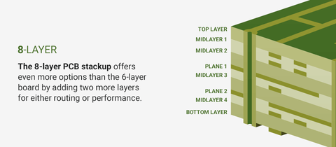
8-Layer
The 8-layer PCB stackup offers even more options than the 6-layer board by adding two more layers for either routing or performance. It is also the first board listed that can achieve all five objectives for multilayer PCB design.
Typical 8-layer PCB stackups feature the power and ground layers in the center, offering good capacitance between layers as well as a separation between the second and third signal planes to protect signal integrity. This results in a common 8-layer PCB stackup that looks like the following:
- Signal layer 1
- Prepreg
- Ground plane
- Core
- Signal layer 2
- Prepreg
- Power plane
- Core
- Ground plane
- Prepreg
- Signal layer 3
- Core
- Power plane
- Prepreg
- Signal layer 4
These PCBs do not feature more than four signal planes — instead of added signal planes, these PCBs feature more ground and power planes to optimize EMC performance. While this may seem less than optimal considering the additional cost of manufacturing an 8-layer over a 6-layer PCB, there is a good reason to choose this option. While 8-layer PCBs are more expensive than 2-, 4- and 6-layer options, the percentage increase in the cost of an 8-layer board over a 6-layer board is less than the percentage increase in the cost of a 6-layer board over a 4-layer board. The smaller increase makes it much easier to justify the cost increase for the improved emissions performance.
10-Layer
If your design requires six routing layers, then you should look into a 10-layer board. A 10-layer PCB stack features six signal layers and four planes, with tight coupling between the signal and return planes. Typical 10-layer designs are arranged into the following:
- Signal layer 1
- Ground plane
- Signal layer 2
- Signal layer 3
- Power plane
- Ground plane
- Signal layer 4
- Signal layer 5
- Power plane
- Signal layer 6
For this arrangement, high-speed signals are typically routed on the internal signal layers. When stacked and routed appropriately, this setup can provide both excellent signal integrity and great EMC performance. It is not recommended to replace any of the grounding or power planes with additional signal layers, as this can result in poor performance.