Key Takeaways
- PCB assembly and soldering complete the physical building of a circuit by picking, placing, and soldering components onto a board.
- In through-hole technology, leaded or pin-through hole electronic components are soldered to the board to make a circuit.
- Wave soldering is the most common technique used in THT and SMT PCBA.

Printed circuit boards (PCBs) are an essential part of electronics; without PCBs, most electronic devices would just be unusable boxes. PCBs are usually made of fiberglass and held together by epoxy. The PCB assembly and soldering process completes the physical building of the circuit by picking, placing, and soldering components onto the board. The inspection, testing, and feedback following PCB assembly and soldering make PCB manufacturing a successful process. In this article, we will discuss PCB assembly and soldering processes.
PCB Assembly and Soldering
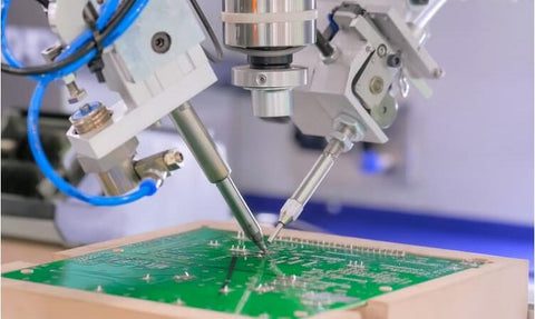
The PCB assembly and soldering process bring a board to a functional prototype. The PCB assembly (PCBA) stages are component placement, soldering, inspection, and, finally, testing. The PCBA process can be either a manual or automated process, which is decided by the manufacturer at each stage.
A Brief Overview of the PCBA Process
PCB design starts with a schematic diagram. From the schematic diagram, the PCB layout is designed. The PCB layout defines the electrical connecting paths, called traces, in the circuit and where to place the components. Once the PCB layout design is approved, it then gets printed.
Fabricated PCBs are pieces of fiberglass material held together by epoxy. Traces made of copper are laid on the board. The components are fixed on the board through a soldering process. The soldering process fixes the components to the place assigned for them using a substance called solder. A PCB with components soldered onto it forms the assembled PCB. Once the components are affixed to the PCB, the board is ready for testing.
There are three technologies used in the PCBA process, which we will discuss next.
PCB Assembly Technologies
There are three key technologies in the PCBA process:
-
Through-hole technology (THT) PCBA process: In through-hole technology, leaded or pin-through hole electronic components are soldered to the board to make a circuit. The leads or terminals of the components are inserted through the holes or pads on the PCB and soldered on the opposite side.
-
Surface-mount technology (SMT) PCBA process: There are two types of pads: through-hole and surface-mount. In PCBs using surface-mount pads, surface-mount devices (SMDs) are soldered to develop the circuit. The soldering process happens on the same surface where the component is placed with the aid of solder paste.
-
Mixed technology PCBA process: As the circuit design becomes complex, it is impossible to stick to only one type of component in a circuit. In PCBs realizing complicated circuits, there are both through-hole as well as surface-mount devices. Such PCBs utilizing mixed components are called mixed technology boards, and the assembly process is a mixed technology PCBA process.
The Steps for Through-Hole Technology PCB Assembly
The sequence of the PCBA process varies with the mounting technology being used. Let’s explore the steps for through-hole technology PCB assembly.
-
Component Placement: In through-hole technology PCBA, the engineer starts by placing components in their respective positions as given in the PCB design files.
-
Inspection and Rectification: After all the components are placed, an inspection is performed on the board. The inspection examines whether the components are placed accurately. If the components are found to be placed inaccurately, such issues are rectified immediately through the rectification step. Inspection and rectification must be completed before the soldering process.
-
Soldering: The next step in the process is soldering, which fixes the components placed to their corresponding pads.
-
Testing: Once the PCB assembly and soldering process is complete, the board is taken for testing. Every PCB board used in an electronic device has gone through this process and passed testing.
There are a variety of soldering techniques available, and we will explore a few below.
Soldering Techniques
Irrespective of the mounting technology used, a soldering process is involved in all PCBA processes. There are many different types of soldering techniques to attach electrical components to a PCB, including:
-
Wave soldering - In wave soldering, a PCB is moved over a wave of hot solder liquid, which solidifies and fixes the components. It is the most common technique used in THT and SMT PCBA.
-
Braze soldering - In braze soldering, metal components are attached through heating. However, this technique melts the metals at the bottom for fitting the filler metal. Braze soldering utilizes the highest temperature and produces the strongest joints.
-
Reflow soldering - The reflow soldering process attaches components to the board using heated soldering paste. The soldering paste in its molten state connects the pads and pins in the PCB.
-
Soft soldering - In the soft soldering technique, a metal space filler made of a tin-lead alloy is heated by an electric torch or gas to fix components to the board. Soft soldering is a popular technique for fixing compact, fragile components to a printed circuit board.
-
Hard soldering - Hard soldering is used for combining metal parts such as copper, brass, silver, or gold at a temperature of about 600°F. Hard soldering produces stronger joints than soft soldering does.
