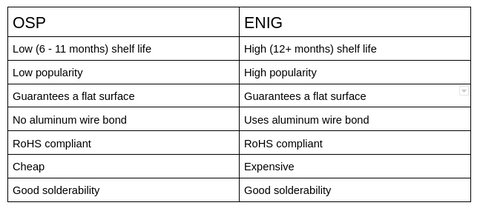
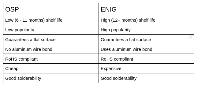
A PCB surface finish is a coating between a bare board PCB and a component. It serves two main purposes — to protect the copper circuitry and ensure solderability. Since there are several types of surface finishes, you may find it hard to find a comprehensive OSP vs ENIG guide. Besides, complicated regulations make the process even harder. These include the WEEE (Waste from Electrical and Electronic Equipment) and the RoHS (Restriction on the use of Hazardous Substances).
OSP
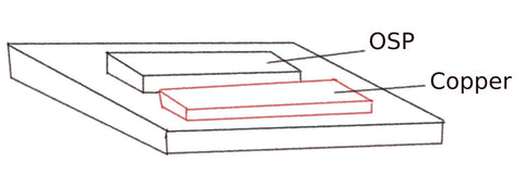
Image Description: OSP
The OSP (Organic solderability preservative) surface finish is an organic type. Therefore, toxins are not present, making them environmentally friendly while retaining their protective nature.
In addition, this finish has a flat surface where you can attach more PCB components. And it’s affordable, just like the HASL process.
OSP is a perfect choice for those who want excellent flatness and a simple manufacturing process.
Image Description: HASL
To apply this PCB surface finish, you’ll need a vertical dip tank or a conveyorized chemical method. The process involves several steps, with rinses in between.
- Cleaning: This step involves cleaning the PCB’s copper surface to remove fingerprints, oil, and other contaminants.
- Topography enhancement: This serves two purposes — to increase the bond between the OSP and the board and reduce oxidation. Besides, for efficient film thickness, you should do micro-stretching at a consistent speed.
- Acid rinse: You should rinse the PCB in a sulphuric acid solution.
- OSP application: Here, you should apply the OSP solution to the PCB.
- Deionization rinse: You should infuse the OSP solution with ions at this stage. By doing so, you’ll enable easy elimination when soldering. Besides, it would help if you rinsed before preservatives accumulate to prevent corrosion due to the availability of more ions in the solution.
- Drying: Lastly, you should dry the PCB after applying the finish.
In brief, note that this process is simple and affordable. However, it’s susceptible, and it can easily cause scratches that may destroy solderability.
ENIG
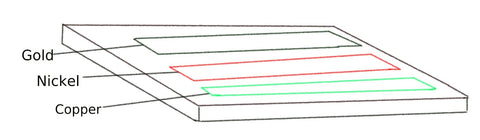
Image Description: ENIG
Although ENIG surface finishing is more expensive than OSP finishing, it produces more quality products. It displays more solderability and holds up under many thermal cycles. Thus, it’s an excellent method for wire bonding.
This method creates two layers of coating — gold and nickel. First, nickel guards the base copper layer against external hazards and ensures the safe attachment of electrical items. On the other hand, gold prevents nickel from corroding.
Thus, ENIG is efficient in cases where you need a high tolerance for PCB components. It provides excellent flatness like OSP. To apply ENIG coating, you must deposit the nickel surface catalyzed by palladium.
ENIG and OSP are similar in that both include micro-etching with rinsing sessions. Below are the steps followed — Cleaning, Micro-etching, First dipping, Activator application, Second dipping, Electroless nickel application, and lastly, Immersion gold application.
OSP vs ENIG