
Grounding in PCB boards holds special place as it can influence the performance greatly. A good time spent on grounding in your PCB design is never wasted. If you don’t focus on grounding the currents in your PCB then your board might run in trouble sooner or later. To avoid that, here are the most important PCB grounding techniques that you should remember the next time you design a PCB.
Ground:
This is the common return path for the flow of current in a circuit. Also it serves as a reference point to measure voltage potential across difference points in a circuit. It’s fair to say ground signal or traces will occupy major portion in a PCB board. Improper grounding can lead to problems such as signal coupling, ground loops, EM noise interference and so on. These problems will negatively affect the performance of your board.
1. USE THE GROUND PLANE:
This technique is popular among designers and one of the effective ways to establish grounding in your PCB boards. It refers to a large plane of copper that carries a return current from different points in PCB. This will a provide large return path for current and serves as a heat sink. Also this will lower impedence across the board, and low cross talk from signal interference.
In general, designers prefer to use bottom layer for ground plane and other signals in the top layer in a 2 layer PCB. Although there may be few signals routed in the ground plane. But it is always advised to keep the number of signal tracks minimum in a ground plane.
In 4 layer PCBs it is advised to dedicate an entire layer for grounding and avoid any other signal traces in that layer. When other signal traces are introduced, it gives rise to a problem called as Ground loop.
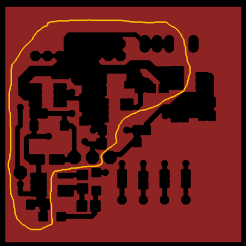
Ground loop occurs when the traces form a circular path for current flow. In an ideal PCB board all points in the ground plane should be in equal potential, however in real PCBs impedance tend to vary across different points even though they are all in the ground plane.
In such cases it will force current flow to bounce back and forth with the ground loop. It’s important to avoid ground loop when using ground planes in your design. This is possible when you are aware of your ground current flow in the board and avoid laying out traces that can create a loop.
Another idea is to use vias to connect with other layers if in case it has a ground plane as well. This will eliminate the ground loop.
2. MORE GROUND CONNECTORS:
Have you ever noticed that PCB boards have ground connector pins more than actually required. This is to avoid impedance mismatch that might occur when connecting the board to another PCBs. This impedance will potentially introduce oscillations in current flow.
As a good practice dedicate 30 to 40 percent of pins in your PCB connector to ground connections. Adding multiple pins can compensate for impedance mismatch and provides additional current path. This will eliminate oscillation.
3. ISOLATE GROUNDS WHEN NECESSARY:
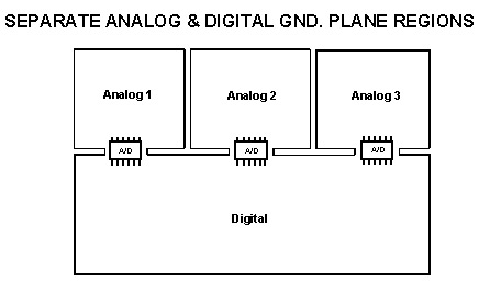
Isolation of Analog and Digital grounds are generally done by creating a partition for analog and digital sections. Later the ground plane of these two partitions will be tied in a single common point. There are also other ways of isolating analog and digital signal lines. You can probably follow the one which fits your application and board space.
4. DECOUPLING:
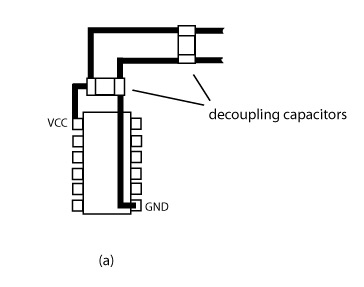
This is a common practice when comes to designing PCBs where a capacitor is connected from power trace to ground trace. Primarily it is used to provide stable power to ICs in a PCB board to eliminate noise in power supplies.
It is also a good grounding technique. Adding decoupling capacitor reduces noise that may occur between power and ground traces. Also it eliminates the EMI interference. Add a dedicated decoupling capacitor to every individual IC in the board and add it as close as possible to chip.
Use identical capacitor of high capacitance with all the chips in board.